

Focused photon energy heating chamber
a technology of focused photon and heating chamber, which is applied in the direction of lighting and heating apparatus, muffle furnaces, furnaces, etc., can solve the problems of crystal defects and slip dislocations in wafers, limited power density of direct radiation, and conventional lamp-based rtp systems with considerable drawbacks. , to achieve the effect of improving the thermal uniformity and ramp rate of the design
- Summary
- Abstract
- Description
- Claims
- Application Information
AI Technical Summary
Benefits of technology
Problems solved by technology
Method used
Image

Examples
Embodiment Construction
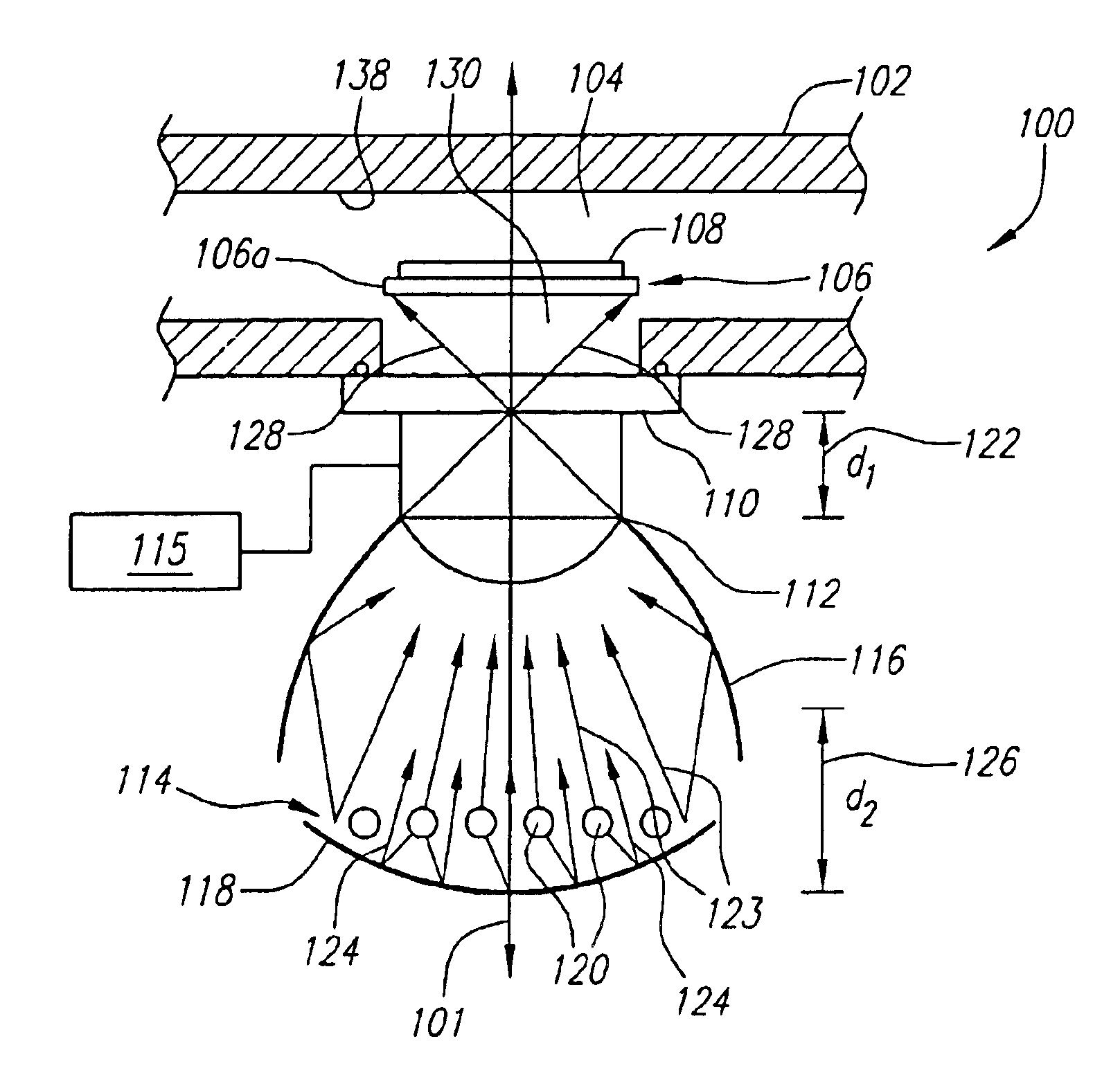
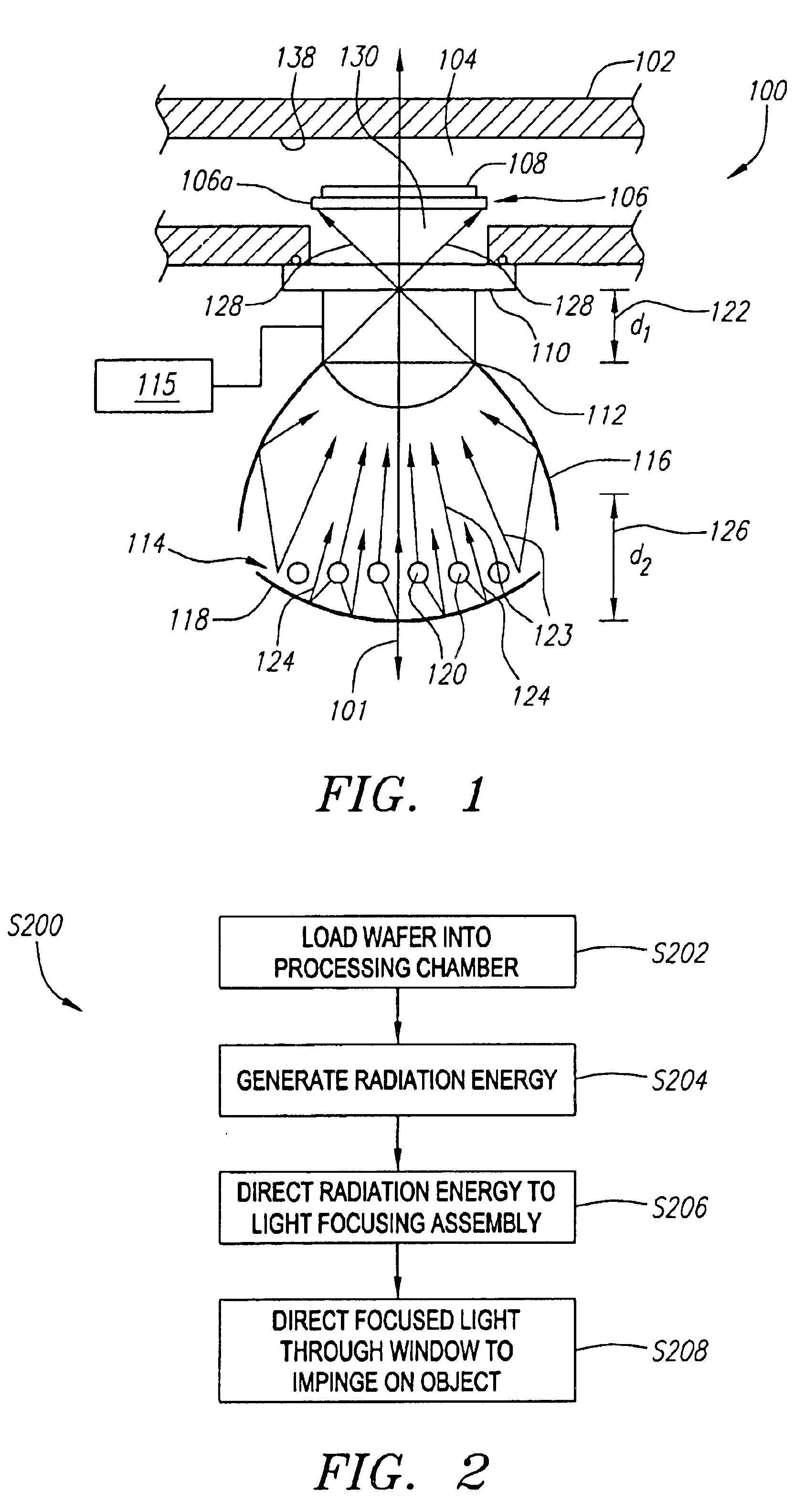
FIG. 1 is a simplified representation of the wafer heating apparatus of the present invention. Heating apparatus 100 includes a processing chamber 102 defining a processing area 104. Optionally, disposed within processing area 104 is a heat absorbing member 106 used to support a single wafer 108 during processing. A window 110 is formed or mounted onto processing chamber 102 to provide optical access along an optical path 101 to processing area 104. External to processing chamber 102 and positioned substantially along optical path 101 are a radiation focusing assembly 112, a radiation source 114, and a strategically positioned radiation reflecting device 118.
It should be understood that optical path 101 is represented by a line segment merely to provide an illustrative representation of the line-of-sight access through window 110 into process chamber 102 upon which some of the components of heating apparatus 100 are generally aligned. Optical path 101 is shown perpendicular to windo...
PUM
| Property | Measurement | Unit |
|---|---|---|
| Temperature | aaaaa | aaaaa |
| Radiation energy | aaaaa | aaaaa |
| Energy | aaaaa | aaaaa |
Abstract
Description
Claims
Application Information