Bump and fabricating process thereof

a technology of bump and fabrication process, which is applied in the direction of semiconductor devices, electrical devices, semiconductor/solid-state device details, etc., can solve the problems of increasing complexity, functionally powerful and highly personalized electronic products, and affecting the final contact with the adhesion layer b>120/b>, so as to increase the mechanical strength of the barrier layer within the bump structure and prevent the bump structure from peeling off the chip

Active Publication Date: 2005-03-08
ADVANCED SEMICON ENG INC
View PDF5 Cites 28 Cited by
  • Summary
  • Abstract
  • Description
  • Claims
  • Application Information

AI Technical Summary

Benefits of technology

Accordingly, one object of the present invention is to provide a bump structure and a fabricating process thereof capable of increasing mechanic

Problems solved by technology

As electronic technologies continue to advance, increasingly complex, functionally powerful and highly personalized electronic products are produced.
Furthermore, the backside of the chip in a flip-chip package may be exposed by desig

Method used


Image

  • Bump and fabricating process thereof
  • Bump and fabricating process thereof
  • Bump and fabricating process thereof

Examples


Embodiment Construction

Reference will now be made in detail to the present preferred embodiments of the invention, examples of which are illustrated in the accompanying drawings. Wherever possible, the same reference numbers are used in the drawings and the description to refer to the same or like parts.

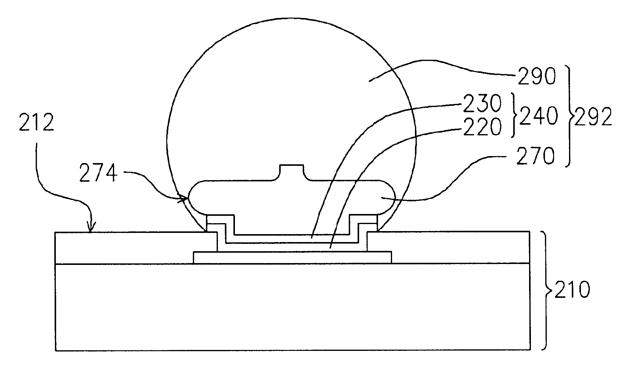
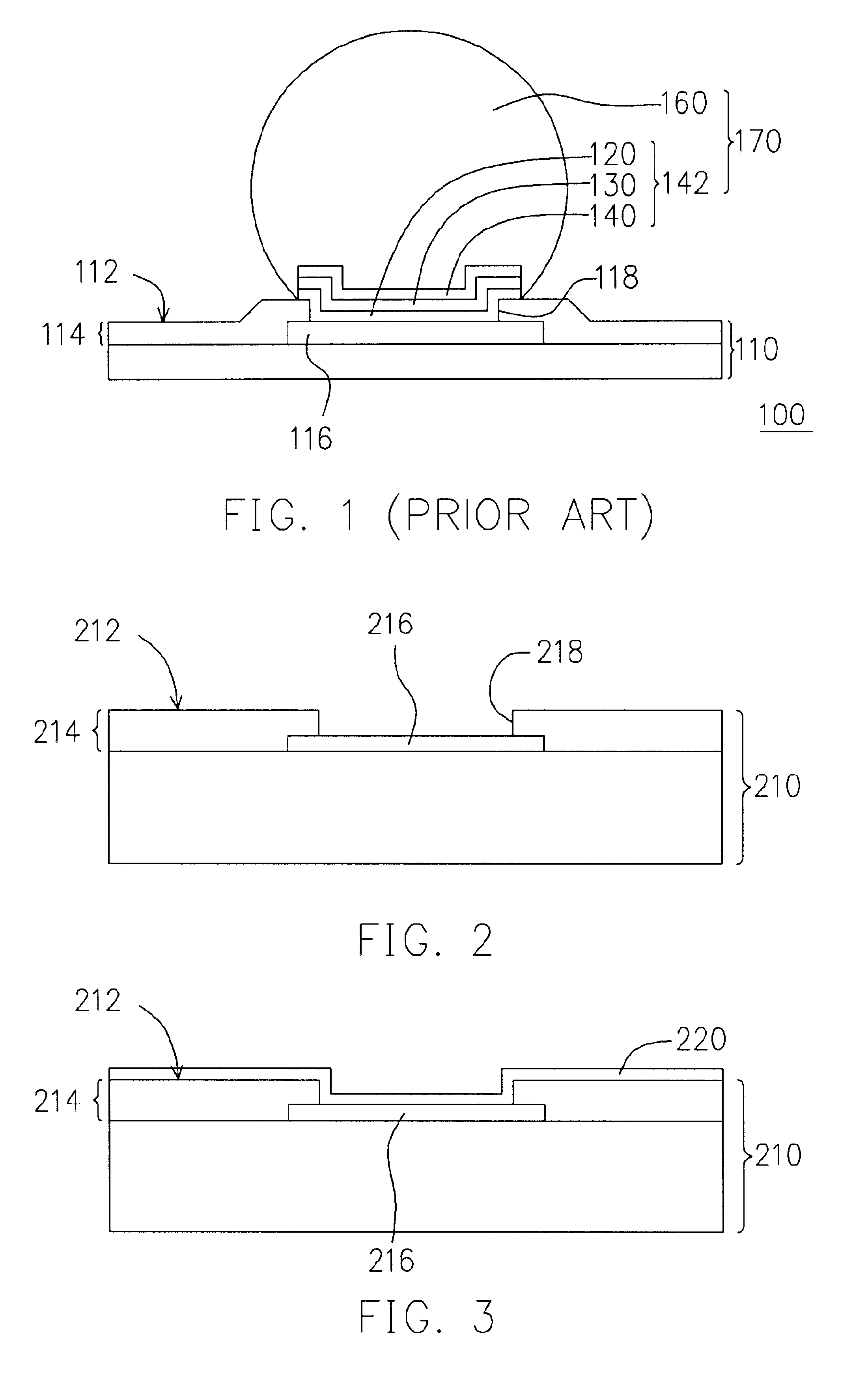
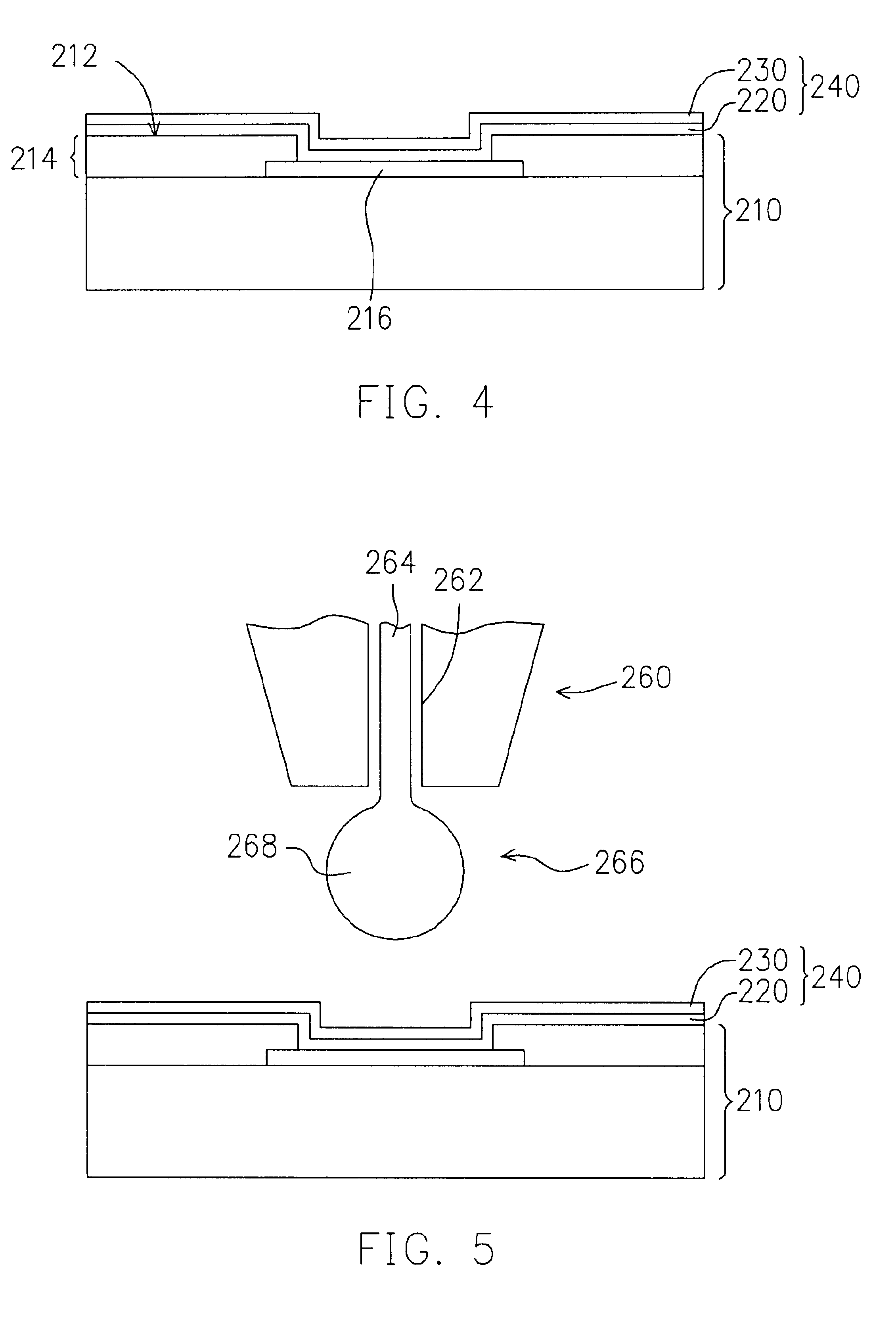
FIGS. 2 to 10 are magnified cross-sectional views showing the progression of steps for fabricating a bump structure according to one preferred embodiment of this invention. First, as shown in FIG. 2, a silicon wafer 210 is provided. The wafer 210 has an active surface 212. The active surface 212 has a passivation layer 214 and a plurality of contact pads (only one is shown in FIG. 2) thereon. The passivation layer 214 has a plurality of openings 218 each exposing a contact pad 216. The passivation layer 214 may be an inorganic compound layer such as a silicon oxide layer or a phosphosilicate glass (PSG) layer. Alternatively, the passivation layer 214 may be a composite layer comprising a stack of the afore...


PUM


Abstract

A bump structure on a contact pad and a fabricating process thereof. The bump comprises an under-ball-metallurgy layer, a bonding mass and a welding lump. The under-ball-metallurgy layer is formed over the contact pad and the bonding mass is formed over the under-ball-metallurgy layer by conducting a pressure bonding process. The bonding mass having a thickness between 4 to 10 μm is made from a material such as copper. The welding lump is formed over the bonding mass such that a sidewall of the bonding mass is also enclosed.

Description

CROSS REFERENCE TO RELATED APPLICATIONSThis application claims the priority benefit of Taiwan application serial No. 91120545, filed on Sep. 10, 2002.BACKGROUND OF INVENTION1. Field of InventionThe present invention relates to a bump and fabricating process thereof. More particularly, the present invention relates to a bump having an improved barrier layer mechanical strength and fabricating process thereof.2. Description of Related ArtIn this information-hungry society, electronic products are used almost everywhere to meet our demands for communication, business transactions, education, recreation and much more. The principle drivers behind all these electrical devices are specially designed integrated circuits. As electronic technologies continue to advance, increasingly complex, functionally powerful and highly personalized electronic products are produced. Rapid progress in design also has brought about the current trend of product miniaturization. Many types of high-density se...

Claims


Application Information

Patent Timeline
IPC IPC(8): H01L21/02H01L21/60H01L23/485H01L23/48
CPCH01L24/03H01L24/05H01L24/11H01L24/13H01L2924/10253H01L2924/01043H01L2924/01033H01L2224/0401H01L2224/05624H01L2224/05666H01L2224/1134H01L2224/13099H01L2224/13111H01L2224/13164H01L2224/78301H01L2924/01005H01L2924/01007H01L2924/01013H01L2924/01014H01L2924/01022H01L2924/01028H01L2924/01029H01L2924/0103H01L2924/01047H01L2924/01049H01L2924/0105H01L2924/01051H01L2924/01074H01L2924/01079H01L2924/01082H01L2924/014H01L2924/14H01L2224/13109H01L2924/01023H01L2924/01024H01L2924/00014H01L2924/00H01L2924/12044
Inventor CHEN, WILLIAM TZE-YOUTONG, HO-MINGLEE, CHUN-CHITAO, SUCHANG, CHIH-HUANGWU, JENG-DAHUANG, WEN-PINCHENG, PO-JEN
Owner ADVANCED SEMICON ENG INC
Why Eureka
Try Eureka