Method for making an electronic component with self-aligned drain and gate, in damascene architecture

a technology of damascus and electronic components, applied in the direction of basic electric elements, electrical equipment, semiconductor devices, etc., can solve the problem that the method of document (2) remains relatively complex however

Inactive Publication Date: 2005-03-15
COMMISSARIAT A LENERGIE ATOMIQUE ET AUX ENERGIES ALTERNATIVES
View PDF10 Cites 28 Cited by
  • Summary
  • Abstract
  • Description
  • Claims
  • Application Information

AI Technical Summary

Benefits of technology

The invention sets out to propose a method for fabricating components which is different to the methods described in the documents indicated above, and with which it is possible to further reduce gate, source and drain resistances.
The layers of contact metal are formed before the replacement of the dummy gate by the final gate. Therefore, in order to prevent the material of the final gate, preferably having low resistivity, from short-circuiting the source and drain, it is necessary to provide for surface insulation or the contact layers in the source and drain regions. This operation could optionally be conducted by depositing a layer of dielectric material. According to one particular aspect of the invention however, the method may comprise superficial oxidation of the metal layers. Oxidation can provide a simple, sure guarantee of electric insulation between source, gate and drain. In addition it avoids any masking operation.

Problems solved by technology

The method of document (2) remains relatively complex however.

Method used


Image

  • Method for making an electronic component with self-aligned drain and gate, in damascene architecture
  • Method for making an electronic component with self-aligned drain and gate, in damascene architecture
  • Method for making an electronic component with self-aligned drain and gate, in damascene architecture

Examples


Embodiment Construction

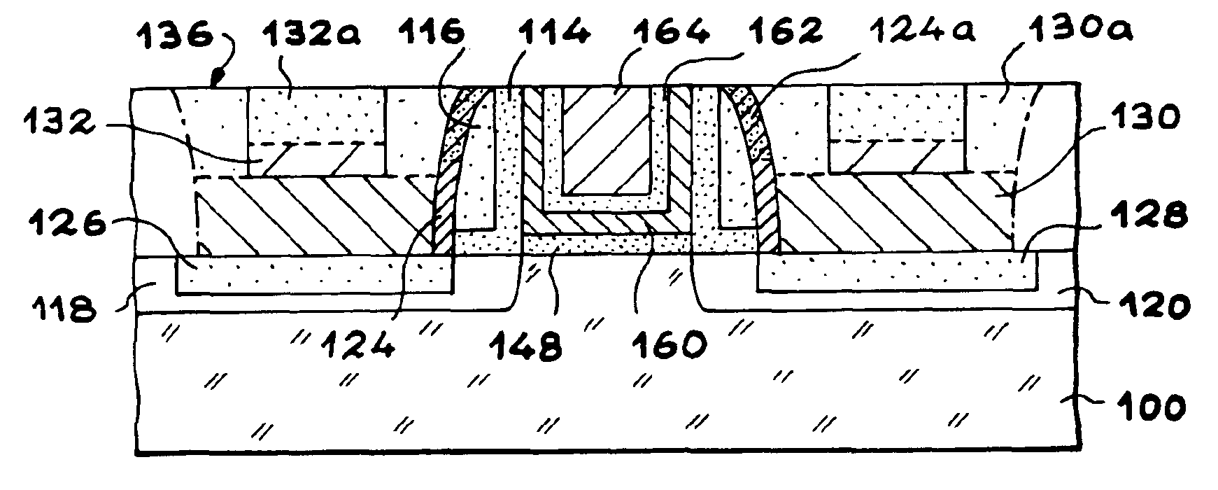
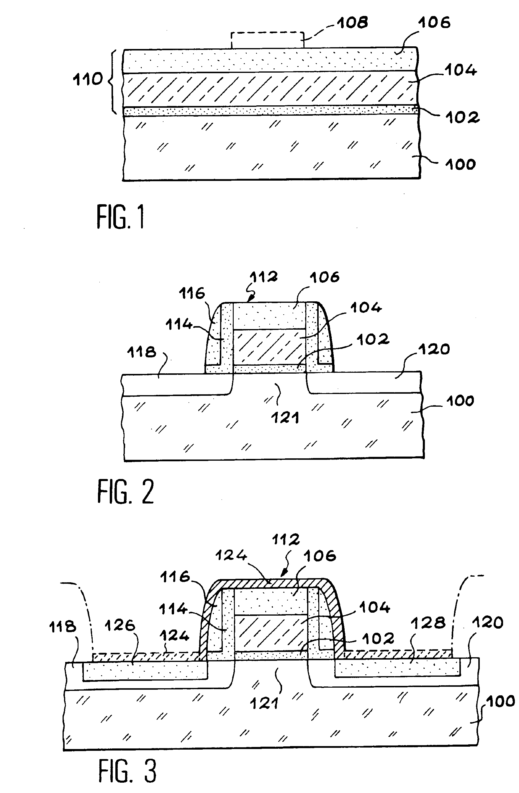
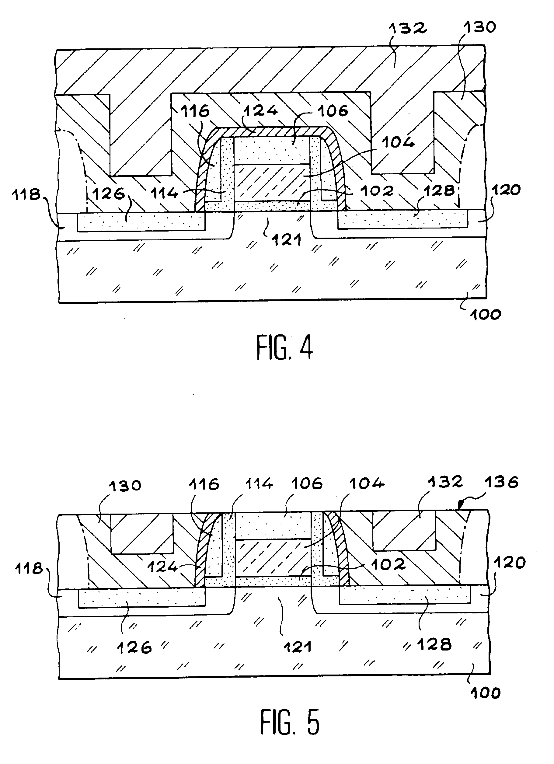
Identical, similar or equivalent parts in the figures described below carry the same numerical references so as to facilitate cross-referencing from one figure to another. Also, even though the following description only concerns the fabrication of components on a solid substrate, in silicon in this case, it is to be emphasized that the methods remain the same for forming components on insulated thin layer substrates, such as substrates of SOI type (Silicon On Insulator).

FIG. 1 shows a silicon substrate 100 whose surface has been oxidized in order to form a silicon oxide layer 102, a so-called pedestal layer.

On layer 102 are successively deposited a layer of polycrystalline or amorphous silicon 104, then a layer of silicon nitride 106. These layers together form a stack 110. The total thickness of layers 104 and 106 is in the order of 100 to 300 nm for example, and substantially corresponds to the thickness of the transistor gate which is finally obtained at the end of the method of...


PUM


Abstract

A method for fabricating an electronic component with a self-aligned source, drain and gate. The method includes forming a dummy gate on a silicon substrate, in which the dummy gate defines a position for a channel of the component. The method also includes at least one implantation of doping impurities in the substrate, to form a source and a drain on either side of the channel, using the dummy gate as an implanting mask, superficial, self-aligned siliciding of the source and drain, depositing at least one contact metal layer having a total thickness greater than a height of the dummy gate, polishing the at least one contact metal layer stopping at the dummy gate, and replacing the dummy gate by at least one final gate separated from the substrate by a gate insulating layer, and electrically insulated from the source and drain. Further, depositing the at least one contact metal layer includes depositing a first metal layer and, above the first metal layer, a second metal layer having a greater mechanical resistance to polishing than the first metal layer. In addition, a thickness of the first metal layer is less than the height of the dummy gate, and a total thickness of the first and second layers is greater than the height of the dummy gate. Further, the first metal is chosen from among tungsten and titanium, and the second metal is chosen from among TaN, Ta and TiN.

Description

TECHNICAL FIELDThe present invention concerns a method for fabricating electronic components with self-aligned source, drain and gate. The components concerned by the invention may be insulated gate transistors such as MOS transistors (Metal Oxide Semiconductor) for example, or electronic memories with a dual gate, that is to say with a command gate and a floating gate.The method of the invention particularly concerns the fabrication of these components on a solid silicon substrate or on a thin layer substrate such as a substrate of SOI type (Silicon on Insulator).The invention finds applications in numerous microelectronic areas, ranging from power switching to hyperfrequency circuits, not forgetting memory circuits.STATE OF PRIOR ARTMethods for producing transistors using self-aligning techniques are known, for example, from documents (1) and (2) whose references are given at the end of this description.Document (1) in particular, concerns the fabrication of a MIS transistor (Meta...

Claims


Application Information

Patent Timeline
Patent Type & Authority Patents(United States)
IPC IPC(8): H01L21/70H01L21/60H01L21/02H01L27/115H01L21/28H01L21/768H01L21/336H01L21/8247H01L29/417H01L29/40H01L29/78
CPCH01L21/28273H01L21/76888H01L21/76897H01L29/66825H01L27/11521H01L29/66545H01L27/115H01L21/28088H01L29/41775H01L29/40114H10B69/00H10B41/30
Inventor DELEONIBUS, SIMON
Owner COMMISSARIAT A LENERGIE ATOMIQUE ET AUX ENERGIES ALTERNATIVES
Why Eureka
Try Eureka