Semiconductor substrate incorporating a neutron conversion layer

a technology of a semiconductor substrate and a neutron conversion layer, which is applied in the direction of semiconductor devices, semiconductor devices, electrical instruments, etc., can solve the problems of helium-3 filled tubes, requiring careful handling, and not being well suited to field operations requiring compact and highly sensitive devices, so as to improve device sensitivity

Active Publication Date: 2005-03-15
THE UNITED STATES OF AMERICA AS REPRESENTED BY THE SECRETARY OF THE NAVY
View PDF1 Cites 42 Cited by
  • Summary
  • Abstract
  • Description
  • Claims
  • Application Information

AI Technical Summary

Benefits of technology

A barrier layer is preferably provided between at least one of the neutron conversion layer and the active semiconductor device layer and the neutron conversion layer and the base substrate to prevent diffusion of the neutron conversion material provided in the neutron conversion layer.
Further, a plurality of trenches may be formed in the active semiconductor device layer to create isolation regions. In such a case, a trench neutron conversion layer may be formed in at least one of the trenches to improve device sensitivity.

Problems solved by technology

These types of conventional neutron detectors are bulky and not well suited for use in field operations requiring compact and highly sensitive devices.
In particular, the helium-3 filled tubes are delicate, require careful handling, and can indicate false positives when abruptly moved or struck.
Lithium metal has been used for this purpose, although the chemical reactivity of the lithium metal tends to lead to shorter detector life.
The use of diode structures, however, in neutron detectors has its own set of drawbacks and limitations.
The internal noise level of an uncooled diode is appreciable, and consequently it is difficult, if not impossible, to measure low background levels of ambient thermal neutrons in the surrounding area.
A typical diode also has a thick semiconductor layer in which charges are collected, and is not sensitive enough to detect single neutron events.
A radiation-induced bit error is known as a soft error if the affected memory cell subsequently responds to write commands.
In contrast, the induced bit error is known as a hard error if subsequent attempts to change the state of the memory cell are ineffective.
These efforts to date, however, have resulted in insensitive detectors primarily because the boron conversion material is not located close enough to the active device layer due to thick overlayers used for interconnection and electrical isolation.
Thus, alpha particles and lithium ions generated by the boron conversion material cannot generate a sufficient charge in the active device layer to cause an SEU.

Method used


Image

  • Semiconductor substrate incorporating a neutron conversion layer
  • Semiconductor substrate incorporating a neutron conversion layer
  • Semiconductor substrate incorporating a neutron conversion layer

Examples


Embodiment Construction

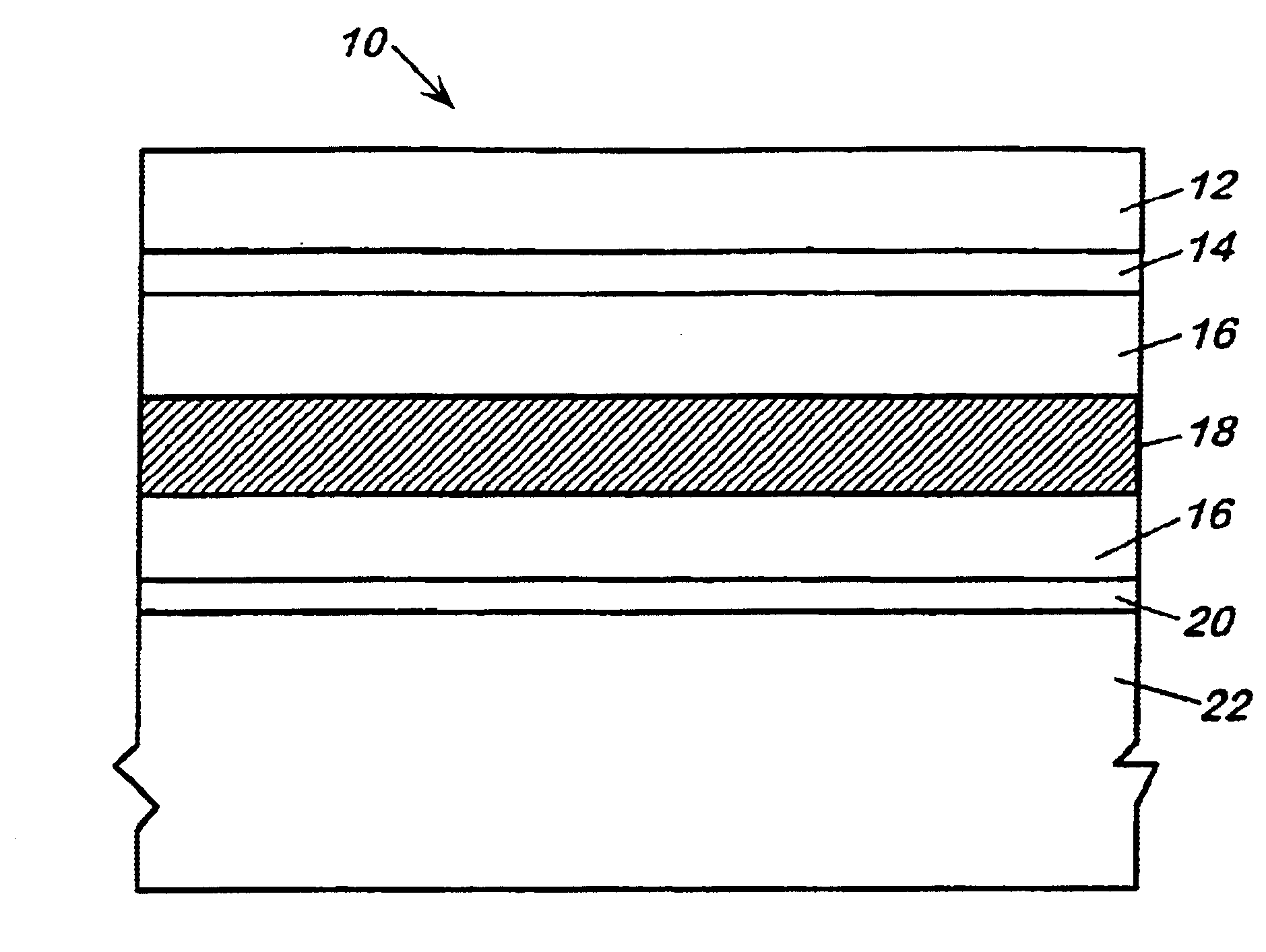
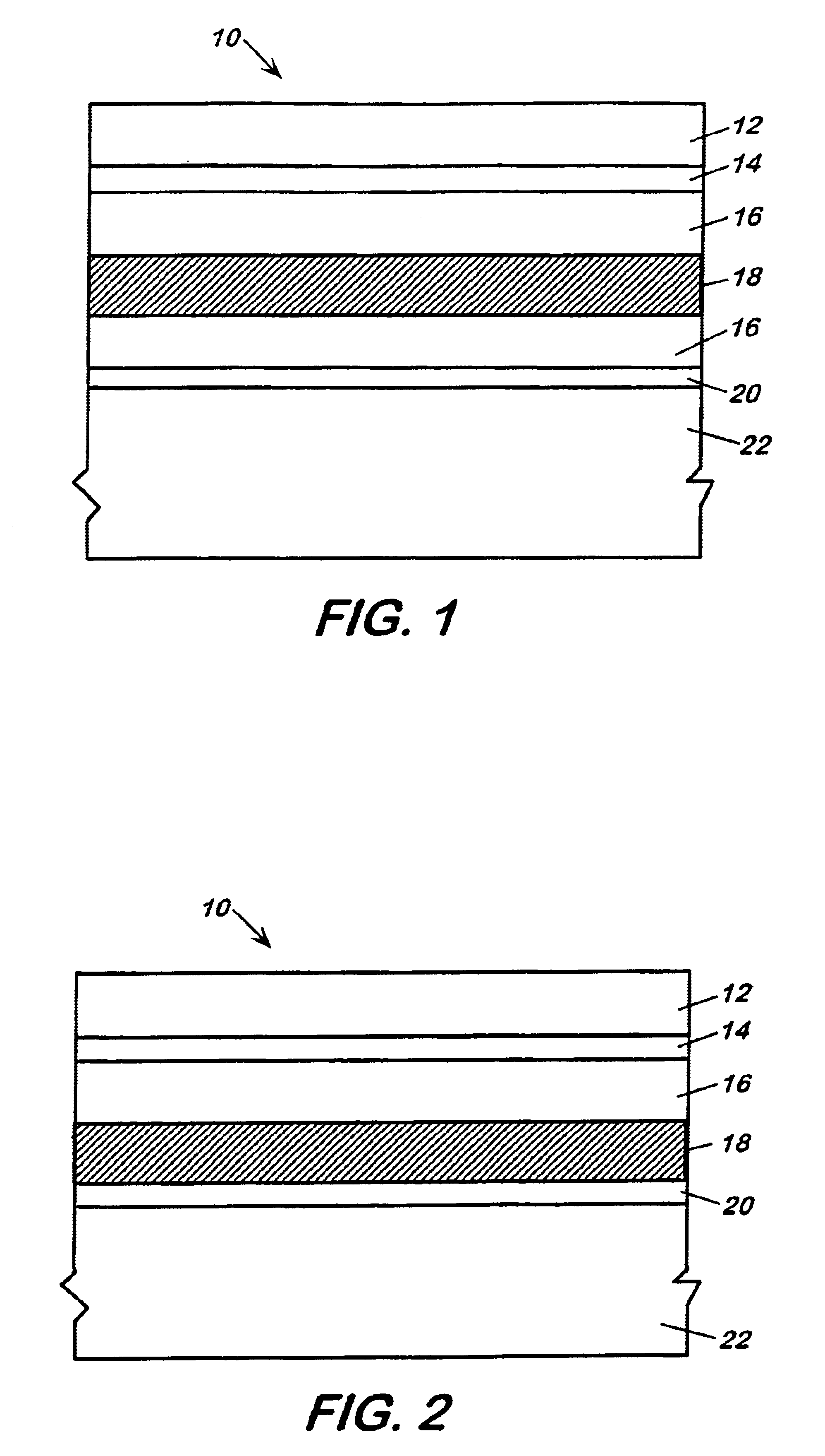
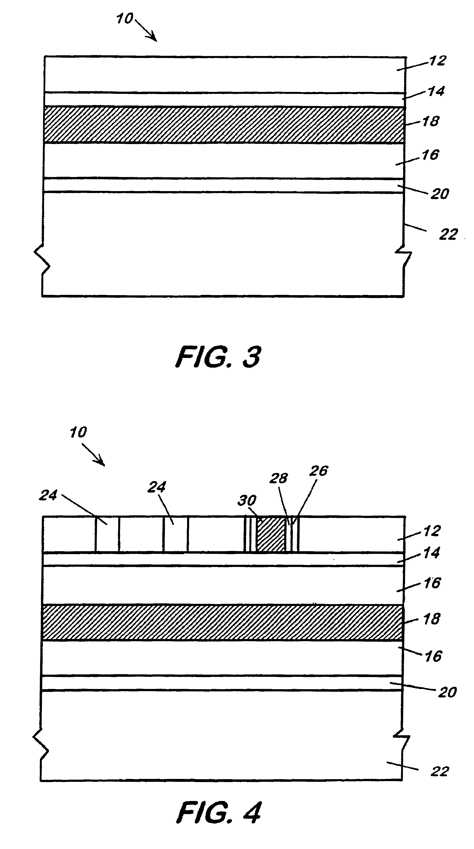
This application hereby incorporates by reference the application entitled “Neutron Detection Device and Method of Manufacture”, assigned NC 84,355, filed on date even herewith. FIG. 1 illustrates a neutron sensitive SOI substrate 10 in accordance with a preferred embodiment of the invention. As shown in FIG. 1, the neutron sensitive SOI substrate 10 includes an active semiconductor (silicon) device layer 12, a top barrier layer 14, an insulating layer 16, a neutron conversion layer 18, a bottom barrier layer 20 and a base (silicon) substrate 22. As will be readily understood with reference to conventional SOI architecture, electronic circuits and circuit elements (including memory cells) are formed in the active semiconductor device layer 12, which may generally range from 10 to 1000 nm in thickness. The insulating layer 16, for example silicon dioxide, constitutes a buried oxide (BOX) that electrically isolates the active semiconductor layer 12 from the base silicon substrate 22. ...


PUM


Abstract

A semiconductor substrate incorporating a neutron conversion layer (such as boron-10) that is sensitive enough to permit the counting of single neutron events. The substrate includes an active semiconductor device layer, a base substrate, an insulating layer provided between the active semiconductor device layer and the base substrate, and a neutron conversion layer provided between the active semiconductor device layer and the base substrate. The neutron conversion layer is located within the insulating layer, between the insulating layer and the base substrate or between the active semiconductive device layer and the insulating layer. A barrier layer is provided between at least one of the neutron conversion layer and the active semiconductor device layer and the neutron conversion layer and the base substrate to prevent diffusion of the neutron conversion material provided in the neutron conversion layer. Further, a plurality of trenches may be formed in the active semiconductor device layer. In such a case, a trench neutron conversion layer is formed in at least one of the trenches to improve device sensitivity.

Description

BACKGROUND OF THE INVENTIONThe present invention is directed in general to semiconductor substrates. The present invention is specifically directed to a semiconductor substrate that includes a neutron conversion layer capable of being utilized for the detection of neutrons. A neutron detection device fabricated in the substrate can be one of many different types including: simple junctions (meta / oxide / metal or p / n junction type), charge-coupled devices (CCDs), and metal-oxide-semiconductor (MOS) integrated circuits.The development of nuclear weapons gave rise to several urgent applications for highly sensitive neutron detectors. The applications include safeguarding nuclear materials and weapons, treaty verification, anti-proliferation, and the recovery of lost military payloads. More recently, however, the need to guard against nuclear smuggling, the potential of a radiological weapon (so called “dirty” bombs), and terrorist acts, has given rise to an urgent need to perform neutron...

Claims


Application Information

Patent Timeline
Patent Type & Authority Patents(United States)
IPC IPC(8): H01L27/14H01L29/66H01L29/84G01T3/08H01L31/0248H01L31/08H01L31/115
CPCG01T3/08H01L31/115H01L31/085H01L31/0248
Inventor HUGHES, HAROLD L.
Owner THE UNITED STATES OF AMERICA AS REPRESENTED BY THE SECRETARY OF THE NAVY
Why Eureka
Try Eureka