Electro-mechanically polished structure

a technology of electromechanical polishing and electromechanical polishing, which is applied in the direction of electrical equipment, semiconductor devices, semiconductor/solid-state device details, etc., can solve the problems of significant problems, etching and/or polishing platinum, and the use of platinum as the material of choice for capacitor electrodes, etc., to achieve the effect of increasing the processing accuracy of metal surface polishing

Inactive Publication Date: 2005-03-15
ROUND ROCK RES LLC
View PDF78 Cites 27 Cited by
  • Summary
  • Abstract
  • Description
  • Claims
  • Application Information

AI Technical Summary

Benefits of technology

The present invention provides a method for patterning metal surfaces employed in the formation of various semiconductor device components, such as capacitors, as well as a method for increasing processing accuracy in polishing metal surfaces.

Problems solved by technology

The use of platinum as the material of choice for capacitor electrodes, however, poses significant problems.
One problem arises from the difficulty of etching and / or polishing platinum and the corresponding need to precisely etch the platinum into the shape of the desired capacitor electrode.
Noble metals such as platinum, however, are not highly reactive with conventional chemical etchants.
This wet etching, however, offers a very low degree of precision.
Consequently, wet etching is not accurate enough for many fine pattern processes, such as patterning DRAM devices, rendering it difficult to perform submicron patterning of platinum electrodes.
While the ion beam milling process is used to define and form high resolution patterns from a blanket platinum layer, this process is typically not selective to many masking materials as well as to the layers underlying the platinum layer.
Further, ion beam milling processing removes most materials at about the same rate, making process control very difficult as the ion beam may remove material underlying a protective mask as well as unwanted material.

Method used


Image

  • Electro-mechanically polished structure
  • Electro-mechanically polished structure
  • Electro-mechanically polished structure

Examples


Embodiment Construction

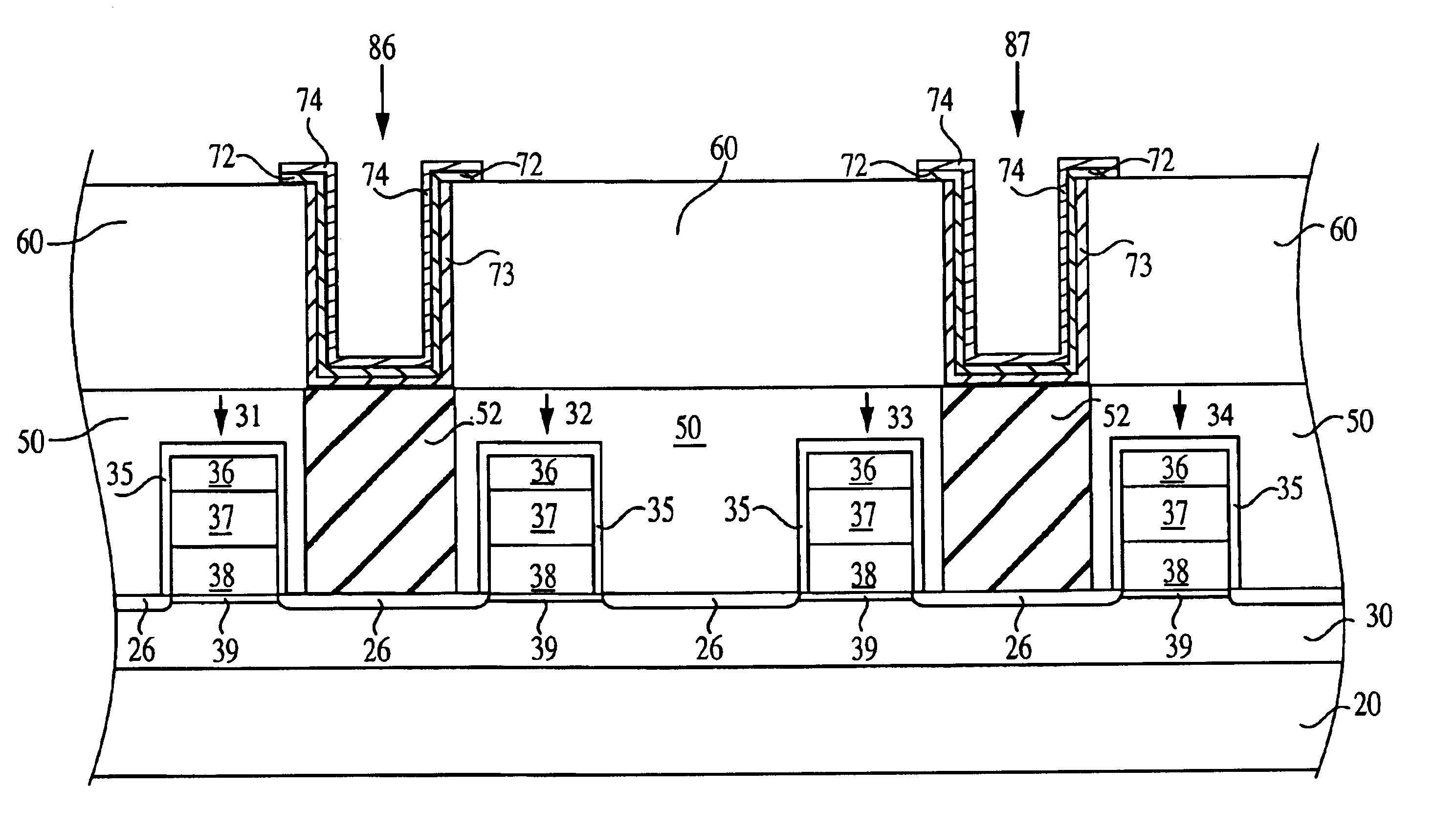
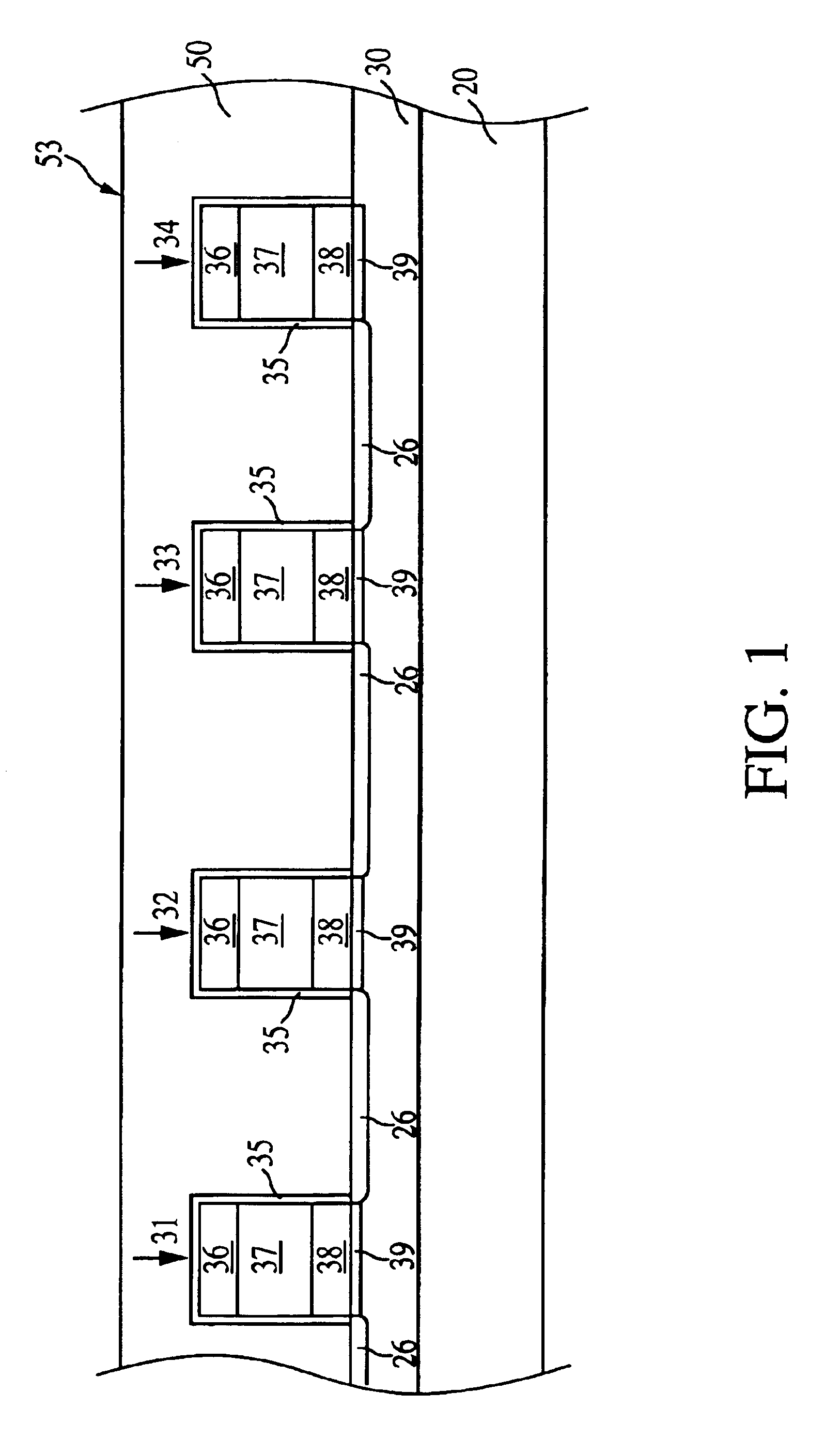
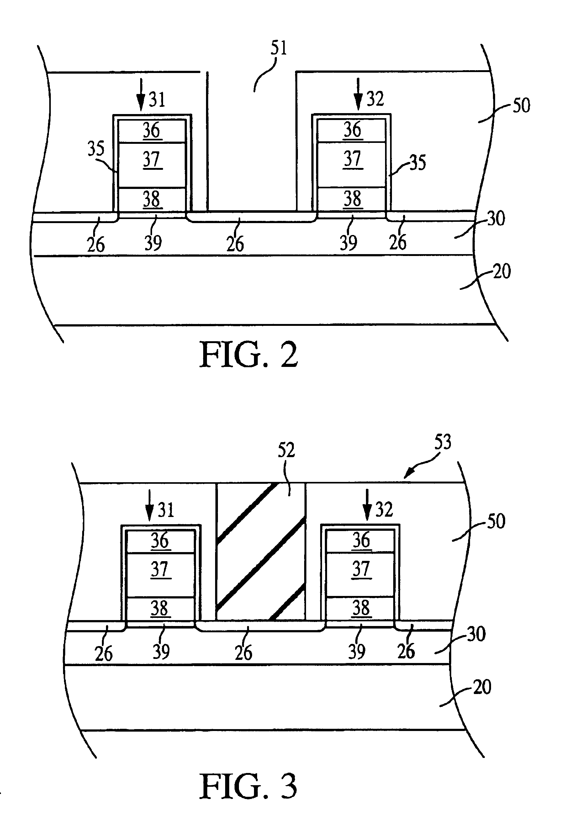
The present invention will be described as set forth in the preferred or exemplary embodiments of the detailed description and as illustrated in FIGS. 1-13. These embodiments are described with sufficient detail to enable those skilled in the art to practice the invention, and it is to be understood that other embodiments may be employed, and that structural, logical, and electrical changes may be made without departing from the spirit or scope of the present invention.

The term “substrate” used in the following description may include any semiconductor-based structure that has an exposed silicon surface. Structure must be understood to include silicon, silicon-on insulator (SOI), silicon-on sapphire (SOS), doped and undoped semiconductors, epitaxial layers of silicon supported by a base semiconductor foundation, and other semiconductor structures. The semiconductor need not be silicon-based. The semiconductor could be silicon-germanium, germanium, or gallium arsenide. When reference...


PUM

PropertyMeasurementUnit
thicknessaaaaaaaaaa
thicknessaaaaaaaaaa
thicknessaaaaaaaaaa

Abstract

A method of patterning a metal surface by electro-mechanical polishing is disclosed. A metal surface is placed in fluid communication with an abrasive surface of a pad. The two surfaces are moved relative to each other, in acidic fluid which contains abrasive particles. An electrical circuit is formed between the metal surface and abrasive pad and a current is supplied to the circuit. The patterned surface then is processed into a useful feature such as a bottom electrode for a DRAM capacitor.

Description

FIELD OF THE INVENTIONThe present invention relates to a method of electro-mechanical polishing (EMP) surfaces, especially surfaces of platinum container structures, during semiconductor device fabrication.BACKGROUND OF THE INVENTIONAs the dimensions of semiconductor devices continue to decrease, there is a need for high resolution patterning of device features. The need for smaller surface area for components, such as capacitors or transistors, along with the requirement to maintain high-reliability electrical connections, have led researchers to seek new materials and methods for fabricating semiconductor components.For example, promising candidates for materials for capacitor electrodes used in integrated circuits memory structures include noble metals, i.e., platinum (Pt), palladium (Pd), iridium (Ir), ruthenium (Ru), rhodium (Rh), osmium (Os), silver (Ag) and gold (Au), as wells as their oxides, e.g., ruthenium oxide (RuO2), indium oxide (IrO2) or osmium oxide (OsO2). The above...

Claims


Application Information

Patent Timeline
Patent Type & Authority Patents(United States)
IPC IPC(8): H01L21/02H01L21/321H01L21/288H01L21/3213B23H5/08
CPCB23H5/08H01L21/3212H01L21/32134H01L21/2885
Inventor LEE, WHONCHEEMEIKLE, SCOTT
Owner ROUND ROCK RES LLC
Why Eureka
Try Eureka