Stacked hybrid semiconductor-magnetic spin based memory

a hybrid memory and semiconductor technology, applied in galvano-magnetic hall-effect devices, pulse techniques, instruments, etc., can solve the problems of inability to manufacture reliable cells on a submicron scale, the size of dram memory cells is not decreasing as rapidly, and the capacitors have not benefited from similar technological gains, etc., to achieve superior signal to noise readout characteristics and greater isolation

Inactive Publication Date: 2005-03-22
SEAGATE TECH INT
View PDF37 Cites 24 Cited by
  • Summary
  • Abstract
  • Description
  • Claims
  • Application Information

AI Technical Summary

Benefits of technology

An object of the present invention therefore is to provide a new, nonvolatile, smaller storage element with greater isolation and superior signal to noise readout characteristics, for use as the storage cell in a [random access] memory circuit.
The hybrid memory cell has specific advantages over MRAM. The readout voltage is larger, with a superior signal to noise characteristic, so that read times are much shorter. The bias current is smaller so that the power dissipated during the read cycle is much less. The packing density is greater because the magnetoresistive element in the MRAM cell is larger and because each MRAM cell requires two elements.

Problems solved by technology

While FETs have benefited from advances in processing techniques so that they can be fabricated with dimensions smaller than a micron, capacitors have not benefited from similar gains in technology and it is still necessary for capacitors to have dimensions of order one micron or larger in order to hold the necessary charge.
Thus, the size of DRAM memory cells is not decreasing as rapidly as processing technology would allow, and one significant drawback of DRAM is that reliable cells might never be fabricated on a submicron scale.
Furthermore, the necessity of comparing capacitance with that of dummy cells requires the fabrication of dummy cells which take up extra space on the chip.
A second disadvantage, for some cell designs, is that the read process drains whatever charge is stored on the capacitor.
This phenomenon is known as “destructive readout” because the read process destroys the state of the cell (capacitor), and a rewrite circuit must be provided to rewrite the memory after every read.
The rewrite circuit takes up space on the chip and the rewrite process can lengthen the amount of time of the read cycle.
A third weakness is that the capacitor plate of any cell is never perfectly isolated.
There is always some finite impedance to ground which permits the charge to leak from the capacitor, and in this process the memory is also lost.
A fourth problem with DRAM is that a particle radiation, either from background sources or from contaminants on the chip, can cause a spurious discharge of the capacitor and give a false reading.
This is one of the largest error mechanisms limiting the reliability of DRAM.
This structure has similar limitations to the oxide dielectric capacitors described above: the read process is destructive, the cells are susceptible to α particle radiation.
Finally, the ferroelectric material degrades with time so that the cell is incapable of sustaining an infinite number of read and write cycles.
However, the signal to be sensed is quite small and the signal to noise ratio is poor.
Power dissipation is relatively large during readout because relatively large currents must be applied to long, resistive lines.
Finally, errors can be introduced during readout if the bias current tips the magnetization into an unstable state.
Since this cell requires the fabrication of two resistors, substantial space is used.
The drawback of this approach is that each cell requires a significant amount of space on a chip, and the complicated fabrication procedures required for circuits composed of numerous transistors will drive up the cost per bit of the memory.
The disadvantage here is that passive circuit elements, in particular resistors and capacitors, require substantial space on a chip.
Thus, the majority of cell area is occupied by passive elements and packing densities are limited.
Furthermore, cell isolation is not very efficient and the readout voltage can be degraded during transmission to the sense circuit, resulting in higher noise and lower readout sensitivity.

Method used


Image

  • Stacked hybrid semiconductor-magnetic spin based memory
  • Stacked hybrid semiconductor-magnetic spin based memory
  • Stacked hybrid semiconductor-magnetic spin based memory

Examples


first embodiment

of Hybrid Memory Cell with Magnetic Spin Transistor and Associated Fet

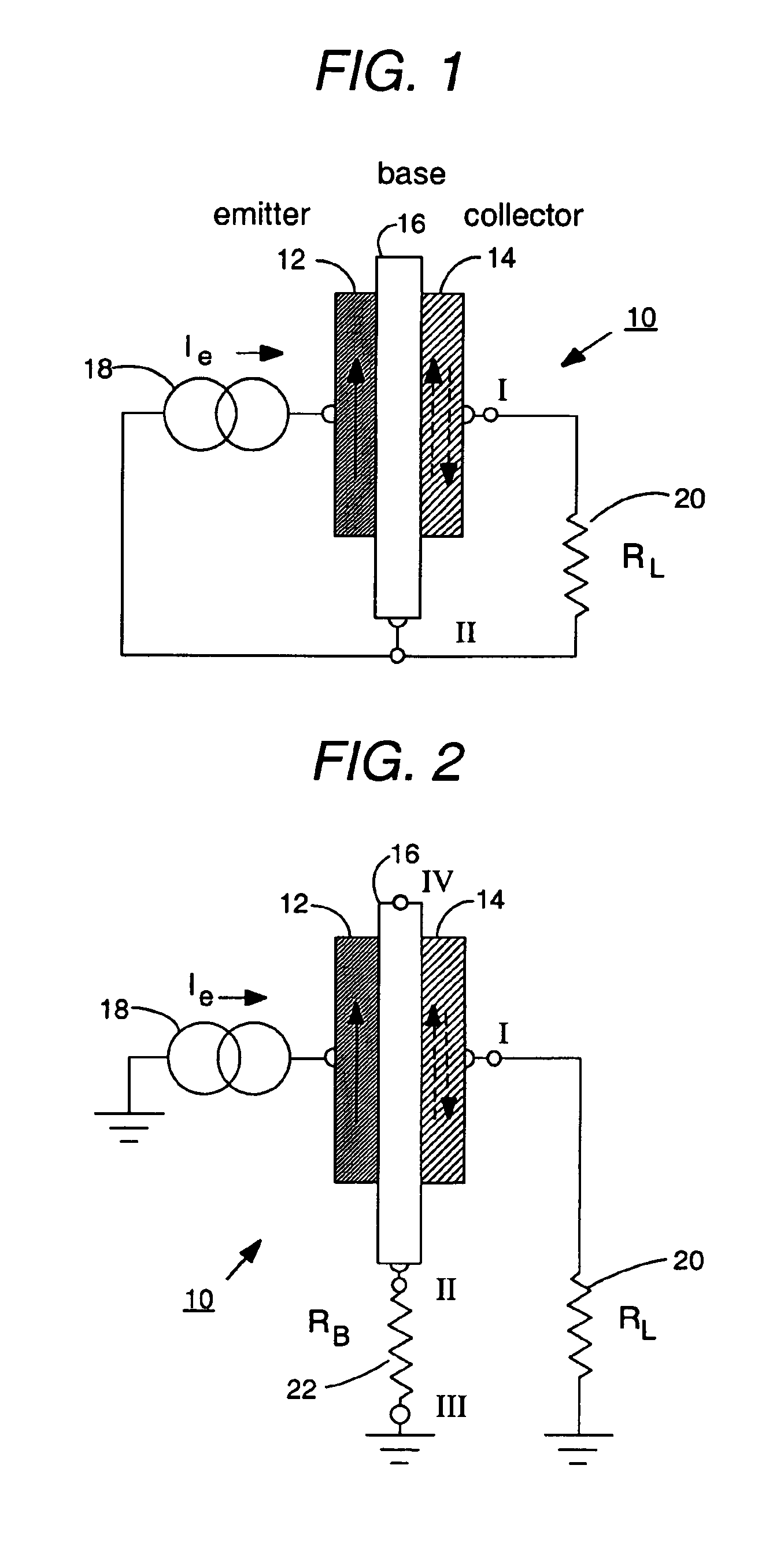
A first embodiment of a spin transistor hybrid memory cell 400 as it may be used in a memory array is shown schematically in FIG. 4. Write wires are not shown in the figure and write functions are performed in the same manner as described above. A description of the read operation now follows. The cell 400 is denoted by the dotted line surrounding the two circuit elements: a spin transistor 10 is the storage element and a FET 420 [a bjt could also be used] is hereafter referred to as a select transistor. A read pulse IR applied to the input terminal 402 provides the bias current for reading the state of the spin transistor, e.g. a positive output voltage [with respect to ground] representing a “1” or zero [or negative] voltage representing a “0” is developed at the collector 14 and delivered to the FET source 406. The enhancement mode FET 420 performs a cell select function in the same way as done in a typical con...

second embodiment

of Hybrid Memory Cell

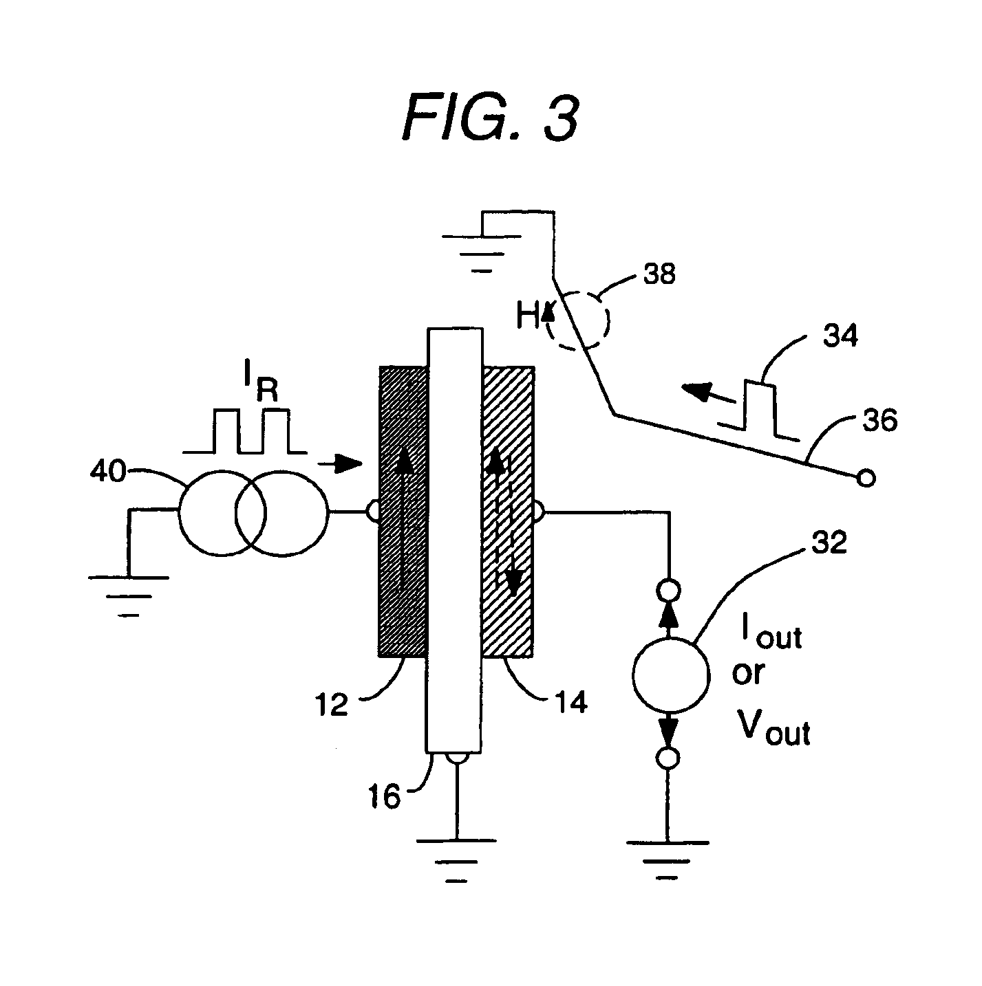
A second embodiment of a spin transistor hybrid memory cell 500 is shown schematically in FIG. 5. This embodiment is especially suitable for designs where the [electronic] ground plane of the chip is not constant over a large area and, it is therefore advantageous to provide a voltage reference from each cell. In addition, it might be desired to connect the common read line to a column of magnetic spin transistors in series rather than in parallel [i.e. connect the ground of one cell to the input of the next]. In this case it would be necessary to provide a reference [ground] for each cell.

When the ground plane is not constant it may be difficult to utilize a bipolar output. The bipolar output of the spin transistor can be easily offset, however, by manipulating parameters such as RB and the geometry of the device. For example, it is convenient to offset the output by choosing RB =RS so that the voltage output is 2* IR*RS for a “1” and 0 for a “0.” In this case ...

third embodiment

of Hybrid Memory Cell with Bipolar Output and Configurable Offset

A third embodiment of a spin transistor hybrid memory cell 600, conceptually very similar to the second, is presented in FIG. 6. If the ground plane is not constant over a large area of the chip but the use of a bipolar sense circuit is still desired, this third embodiment can be used. Here the reference voltage VR is taken from the base, at a location of the base that is remote from the base—collector interface and which is independent of the base resistance RB. This figure demonstrates that a variation of sample geometry, as well as selection of an appropriate value for RB, can be used to configure the offset voltage of the spin transistor. In the configuration schematically in FIG. 6, the offset [relative to the reference] is zero regardless of the value of RB, and the output voltage, with respect to this reference, is symmetrically bipolar. As before, a select transistor 620 isolates the collector 14 from the bit l...


PUM

PropertyMeasurementUnit
bias currentaaaaaaaaaa
resistanceaaaaaaaaaa
thicknessaaaaaaaaaa

Abstract

A new nonvolatile hybrid memory cell stacked architecture is provided. The cells are comprised of magnetic spin storage elements stacked on top of each other on a silicon substrate, as well as one or two semiconductor FET isolation elements.

Description

FIELD OF THE INVENTIONThe invention relates generally to hybrid memory devices. In particular, the present invention relates to a new nonvolatile stacked hybrid memory element using magnetic spin devices.BACKGROUND OF THE INVENTIONSolid state Random Access Memories (RAM), presently based on silicon technology, are the most important high-speed, reprogrammable memories in computer systems today. The content of a memory bit is stored in a circuit element called a cell, fabricated in a silicon Integrated Circuit (IC) chip. Each cell can exist in one of two stable states to represent a “0” or a “1.” A word is stored in a particular group of cells in a memory array and can be identified with, and addressed by, a unique numerical address. Thousands to millions of cells can be fabricated in a single Very Large Scale Integrated (VLSI) chip along with additional address decoding and read / write control circuits. Given the address of any word, the memory content of that word can be retrieved d...

Claims


Application Information

Patent Timeline
Patent Type & Authority Patents(United States)
IPC IPC(8): G11C11/56G11C11/16G11C11/18G11C11/02H01L29/66H03K19/02H03K19/18G11B5/37G11B5/33G01R33/06G11C7/00G11C11/00H01L27/22H01L43/06
CPCG01R33/06G01R33/1284G11C11/16G11C11/18H03K19/18H01L27/222H01L27/224H01L27/228H01L29/66984H01L43/06G11C11/5607G11B5/378G11C11/1673G11C11/1653H10B61/10H10B61/00H10B61/22H10N52/00
Inventor JOHNSON, MARK B.
Owner SEAGATE TECH INT
Why Eureka
Try Eureka