Ceramic materials reinforced with single-wall carbon nanotubes as electrical conductors

a carbon nanotube and ceramic material technology, applied in nanoinformatics, energy-based chemical/physical/physico-chemical processes, nanocrystalline ceramics, etc., can solve the problems of brittleness of nanocrystalline ceramics, best conductivity being only available in the center of extrusion, etc., to achieve the effect of reducing processing tim

a carbon nanotube and ceramic material technology, applied in nanoinformatics, energy-based chemical/physical/physico-chemical processes, nanocrystalline ceramics, etc., can solve the problems of brittleness of nanocrystalline ceramics, best conductivity being only available in the center of extrusion, etc., to achieve the effect of reducing processing tim

US6875374B1Inactive Publication Date: 2005-04-05RGT UNIV OF CALIFORNIA

Image

  • Ceramic materials reinforced with single-wall carbon nanotubes as electrical conductors
  • Ceramic materials reinforced with single-wall carbon nanotubes as electrical conductors

Examples


examples

Materials, Equipment, and Experimental Procedures

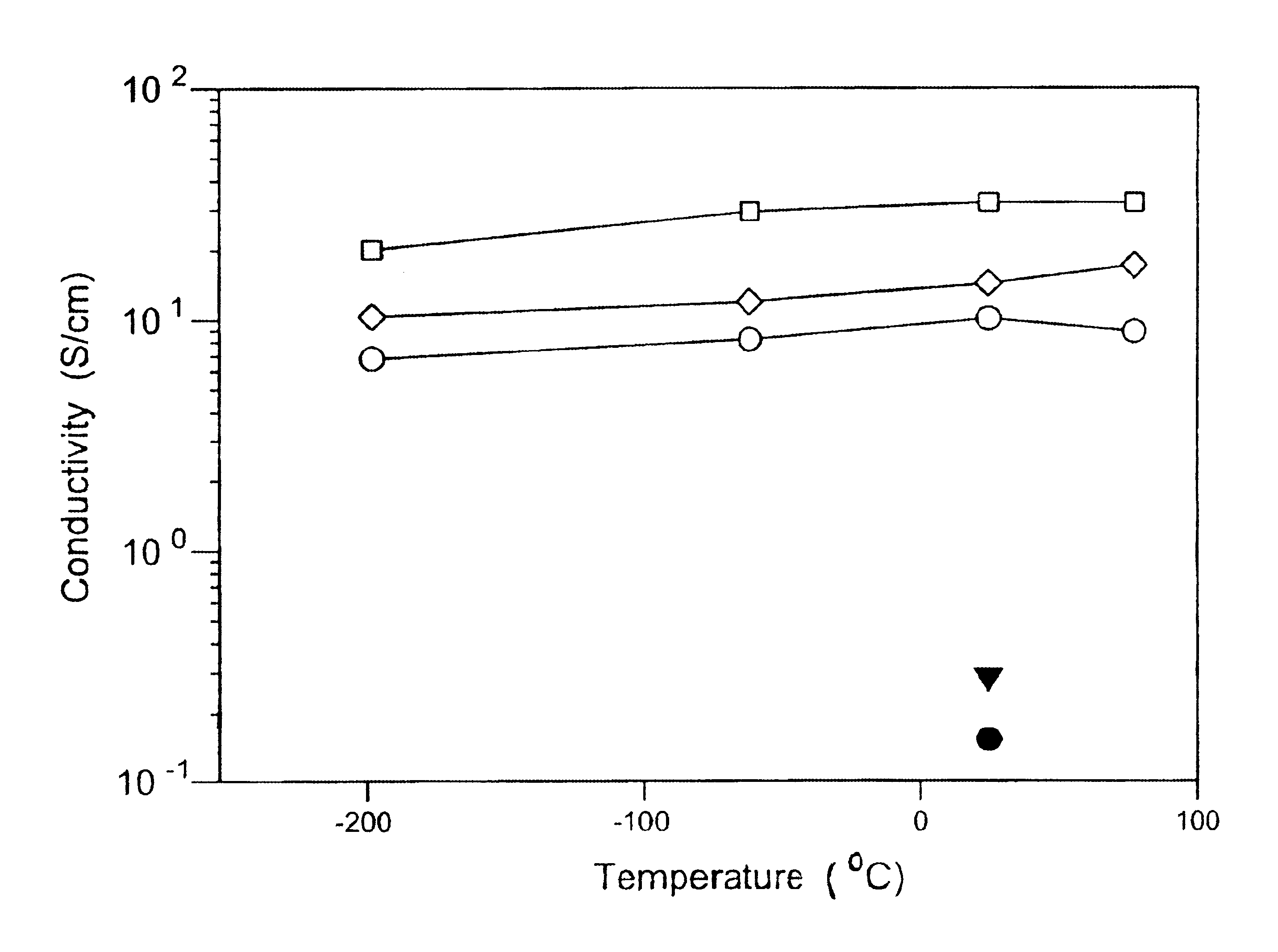
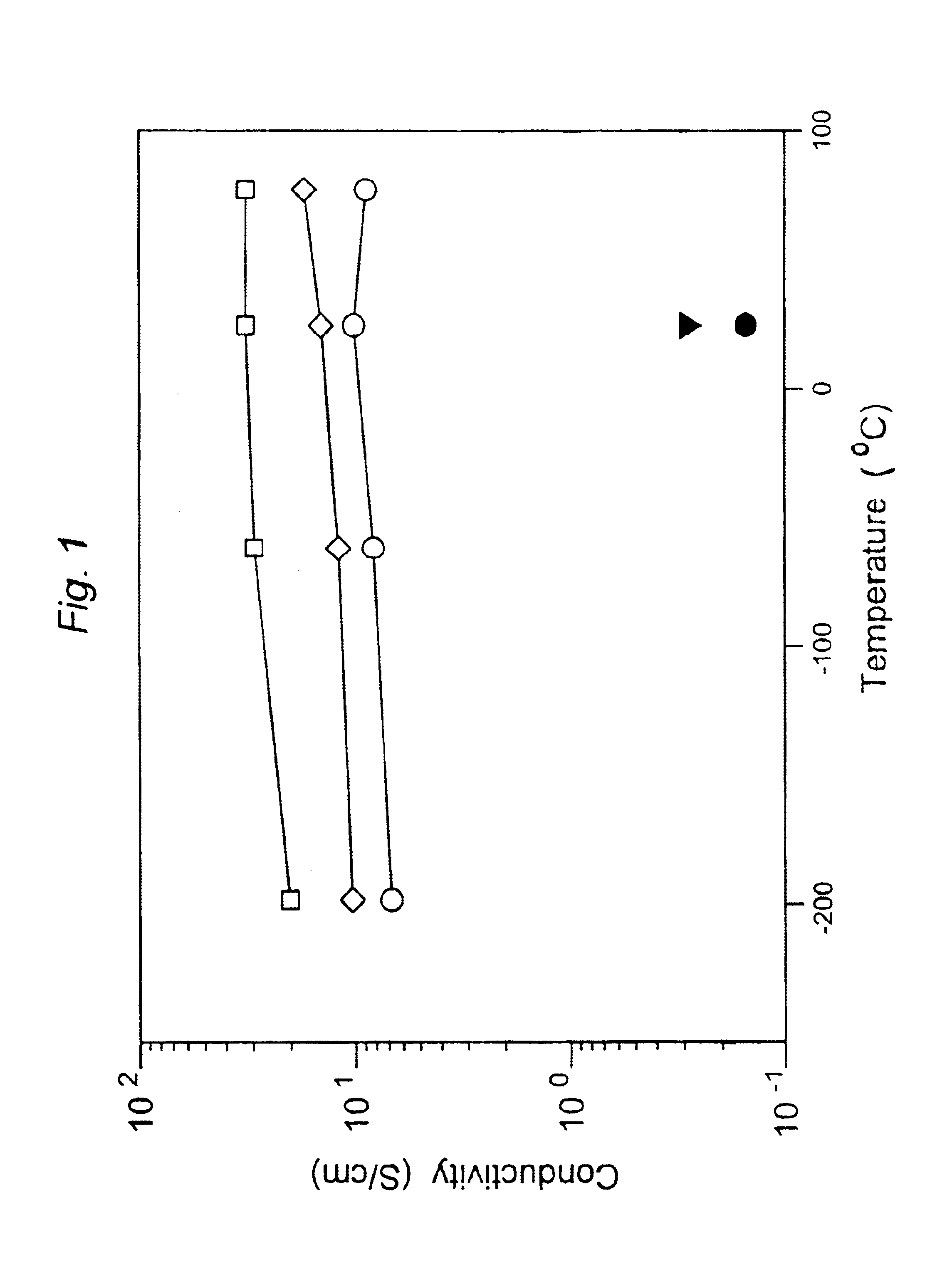
Purified single-wall carbon nanotubes produced by the HiPco process with more than 90% of the catalyst removed were obtained from Carbon Nanotechnologies Incorporated (Houston, Tex., USA). The nanotubes were in paper form, and once obtained were dispersed in ethanol with the assistance of ultrasound. The ceramic material was nanocrystalline alumina powder. A mixture consisting of 80% α-Al2O3 and 20% γ-Al2O3 with particle sizes of 300 nm (40 nm crystallite size) and 20 nm, respectively, was obtained from Baikowski International Corporation (Charlotte, N.C., USA). In addition, γ-Al2O3 with average particle sizes of 15 nm and 32 nm and synthesized by gas condensation was obtained from Nanophase Technologies Corporation (Darien, Ill., USA).

For certain experiments, the alumina or alumina mixture was first mechanically activated by high-energy ball milling prior to being combined with the carbon nanotubes. The high-energy ball milling was p...


PUM

PropertyMeasurementUnit
temperatureaaaaaaaaaa
pressureaaaaaaaaaa
diameteraaaaaaaaaa

Abstract

Composite materials formed of a matrix of fused ceramic grains with single-wall carbon nanotubes dispersed throughout the matrix and a high relative density, notably that achieved by electric field-assisted sintering, demonstrate unusually high electrical conductivity in combination with high-performance mechanical properties including high fracture toughness. This combination of electrical and mechanical properties makes these composites useful as electrical conductors in applications where high-performance materials are needed due to exposure to extreme conditions such as high temperatures and mechanical stresses.

Description

BACKGROUND OF THE INVENTION1. Field of the InventionThis invention resides in the field of electrically conductive ceramics, and incorporates technologies relating to nanocrystalline materials, carbon nanotubes, and sintering methods for densification and property enhancement of materials.2. Description of the Prior ArtThe ability of ceramics to withstand extreme conditions of temperature, mechanical stress, and chemical exposure without failure or with a very low failure rate has led to the use of ceramics in applications that require high-performance materials, such as heat engines, cutting tools, wear and friction surfaces, and space vehicles. In recent years, the use of ceramics has extended into the fields of microtechnology and nanotechnology, since the increasing demands of nano-scale electronics and microelectromechanical systems (MEMS) for example have prompted researchers to investigate the use of ceramics in these areas as well.An unfortunate characteristic of nanocrystal...

Claims


Application Information

Patent Timeline
05 Apr 2005
Publication
US6875374B1
IPC
C04B35/52; C04B35/18; H01B1/14; H01B1/00; C04B35/053; C04B35/119; C04B35/443; C04B35/46; C04B35/488; C04B35/50; C04B35/80; H01L
CPC
B82Y30/00; C04B35/053; C04B35/119; C04B35/443; C04B35/46; C04B35/488; C04B35/50; C04B35/6261
Inventors
ZHAN, GUODONG; KUNTZ, JOSHUA D.