Polarization field enhanced tunnel structures

a technology of enhanced tunnels and tunnels, applied in semiconductor lasers, semiconductor devices, diodes, etc., can solve the problems of high doping requirements, short tunnel distance, and inability to meet one or more of the tunneling conditions, and achieve light or moderate doping levels

Inactive Publication Date: 2005-04-12
BROADCOM INT PTE LTD
View PDF18 Cites 56 Cited by
  • Summary
  • Abstract
  • Description
  • Claims
  • Application Information

AI Technical Summary

Benefits of technology

The invention provides a novel tunnel structure that enables tunnel diode behavior to be exhibited even in material systems in which extremely heavy doping is impossible and only moderate or light doping levels may be achieved.
The first semiconductor layer preferably is doped n-type and the second semiconductor layer preferably is doped p-type. The polarization field preferably enhances a dopant-induced drift field that is produced between the first and second semiconductor layers.
The inventive tunnel heterostructures described herein may be used advantageously in conventional tunnel diode applications (such as microwave oscillators) that depend on the negative differential resistance under forward bias. They can also be used under reverse bias as “leaky” diodes to provide low-voltage drop contacts in material systems in which such contacts are difficult or impossible to achieve. Such low-voltage drop contacts may be used to reduce forward voltages, reduce self-heating and increase power efficiency of semiconductor devices in general, and may be used to reduce the lasing thresholds of semiconductor light-emitting diodes and semiconductor lasers in particular. In addition, the inventive tunnel heterostructure may be used in semiconductor devices (e.g., light emitting semiconductor devices) as a hole source. In this way, the invention allows low mobility and high resistance p-type conductivity channels to be replaced by high mobility and low resistance n-type conductivity channels to improve device performance.

Problems solved by technology

In addition, the tunnel distance must be sufficiently short to enable charge carriers to tunnel across the depletion region with a relatively high probability.
This condition requires very heavy doping levels.
One or more of these tunneling conditions cannot be satisfied in certain semiconductor material systems.
For example, in many semiconductors (especially wide bandgap semiconductors, such as III-V nitride and II-VI semiconductors) heavy doping of the n side or the p side, or both, is difficult or impossible to achieve.
The combined effect of these limitations makes it difficult or impossible to fabricate tunnel diode structures that operate at moderate reverse voltages, much less operate at nearly zero voltage.

Method used


Image

  • Polarization field enhanced tunnel structures
  • Polarization field enhanced tunnel structures
  • Polarization field enhanced tunnel structures

Examples


Embodiment Construction

In the following description, like reference numbers are used to identify like elements. Furthermore, the drawings are intended to illustrate major features of exemplary embodiments in a diagrammatic manner. The drawings are not intended to depict every feature of actual embodiments nor relative dimensions of the depicted elements, and are not drawn to scale.

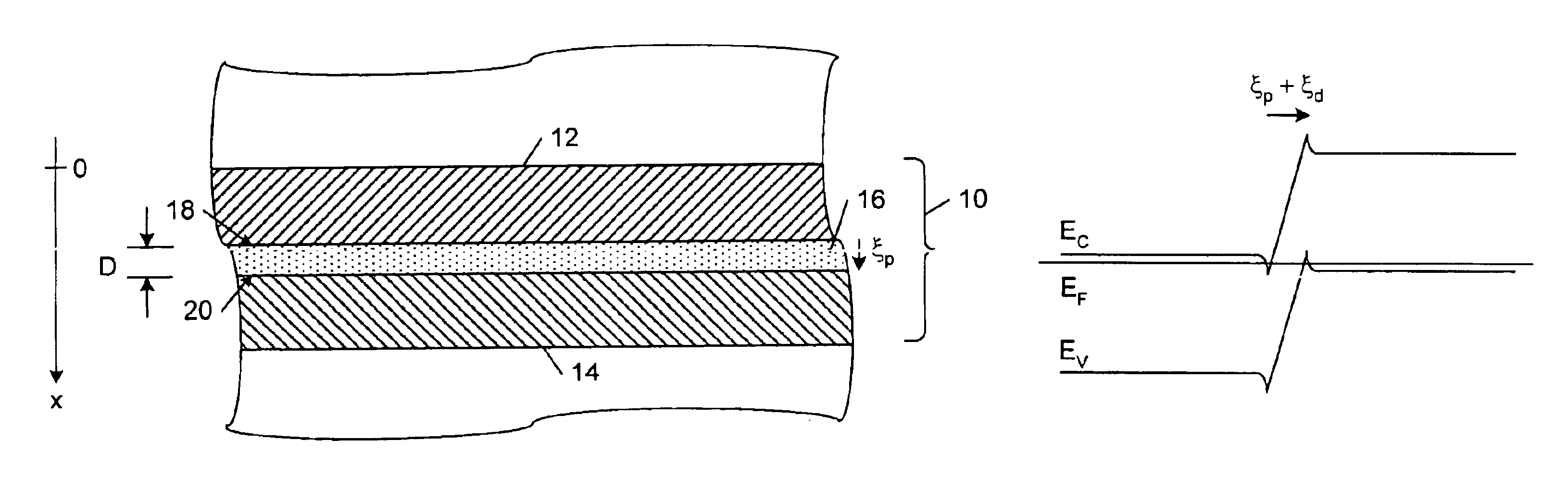
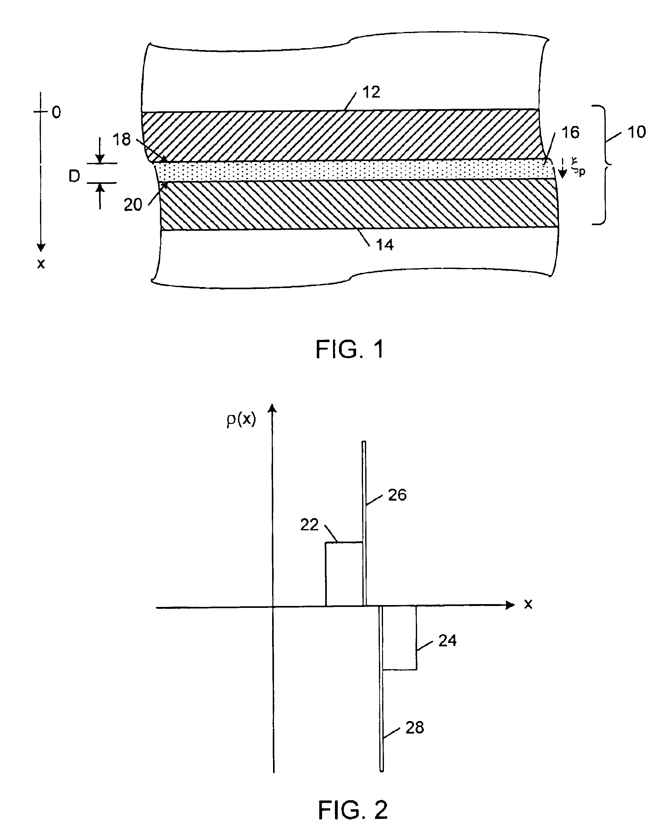
Referring to FIG. 1, in one embodiment, a polarization field enhanced tunnel heterostructure 10 includes a first semiconductor layer 12, a second semiconductor layer 14, and an intermediate semiconductor layer 16. Intermediate semiconductor layer 16 is sandwiched between the first and second semiconductor layers 12, 14, and forms first and second heterointerfaces 18, 20 respectively therewith. First semiconductor layer 12 may be doped n-type, and second semiconductor layer 14 may be doped p-type. Intermediate semiconductor layer 16 has a thickness (D) that is sufficiently thin to enable charge carriers to tunnel through intermed...


PUM


Abstract

A novel tunnel structure is described that enables tunnel diode behavior to be exhibited even in material systems in which extremely heavy doping is impossible and only moderate or light doping levels may be achieved. In one aspect, the tunnel heterostructure includes a first semiconductor layer, a second semiconductor layer, and an intermediate semiconductor layer that is sandwiched between the first and second semiconductor layers and forms first and second heterointerfaces respectively therewith. The first and second heterointerfaces are characterized by respective polarization charge regions that produce a polarization field across the intermediate semiconductor layer that promotes charge carrier tunneling through the intermediate semiconductor layer. In another aspect, the invention features a semiconductor structure having a p-type region, and the above-described heterostructure disposed as a tunnel contact between the p-type region of the semiconductor structure and an adjacent n-type region.

Description

TECHNICAL FIELDThis invention relates to polarization field enhanced tunnel structures.BACKGROUNDMany different tunnel structures have been developed, including tunnel diode structures. A typical tunnel diode is formed from a p-n junction in which both n and p sides are degenerate (i.e., very heavily doped with impurities). The high doping levels bend the conduction and valence bands over a short distance (e.g., on the order of 10 nm, or less) such that conduction band electron states at the Fermi level on the n side are aligned with valence band states at the Fermi level on the p side. This phenomenon allows charge carriers to tunnel across the depletion layer upon application of an arbitrarily small forward or reverse bias across the p-n junction. Beyond a particular forward bias level, the available charge carrier tunnel states do not overlap, resulting in a region of negative differential resistance (i.e., where the current exhibits a decrease in value when the value of the volt...

Claims


Application Information

Patent Timeline
Patent Type & Authority Patents(United States)
IPC IPC(8): H01L29/66H01L29/88H01L33/00H01L29/20H01L29/02H01L33/14
CPCH01L33/14H01L29/88H01L29/2003H01S5/3095
Inventor HUESCHEN, MARK R.
Owner BROADCOM INT PTE LTD
Why Eureka
Try Eureka