MOSgated device with accumulated channel region and Schottky contact

a channel region and mosgate technology, applied in semiconductor devices, semiconductor/solid-state device details, electrical apparatus, etc., can solve problems such as “snap-back” in bvsub>dss, and achieve the effect of limited thermal cycle and deeper penetration of boron

Active Publication Date: 2005-04-12
INFINEON TECH AMERICAS CORP
View PDF3 Cites 16 Cited by
  • Summary
  • Abstract
  • Description
  • Claims
  • Application Information

AI Technical Summary

Benefits of technology

A novel process is also provided for forming the P type gate. Thus, the gate trench is first formed and is then lined with polysilicon. This polysilicon is then implanted with a P type impurity, for example, boron. The trench is then completely filled with p

Problems solved by technology

A limitation found with the above structure

Method used


Image

  • MOSgated device with accumulated channel region and Schottky contact
  • MOSgated device with accumulated channel region and Schottky contact
  • MOSgated device with accumulated channel region and Schottky contact

Examples


Embodiment Construction

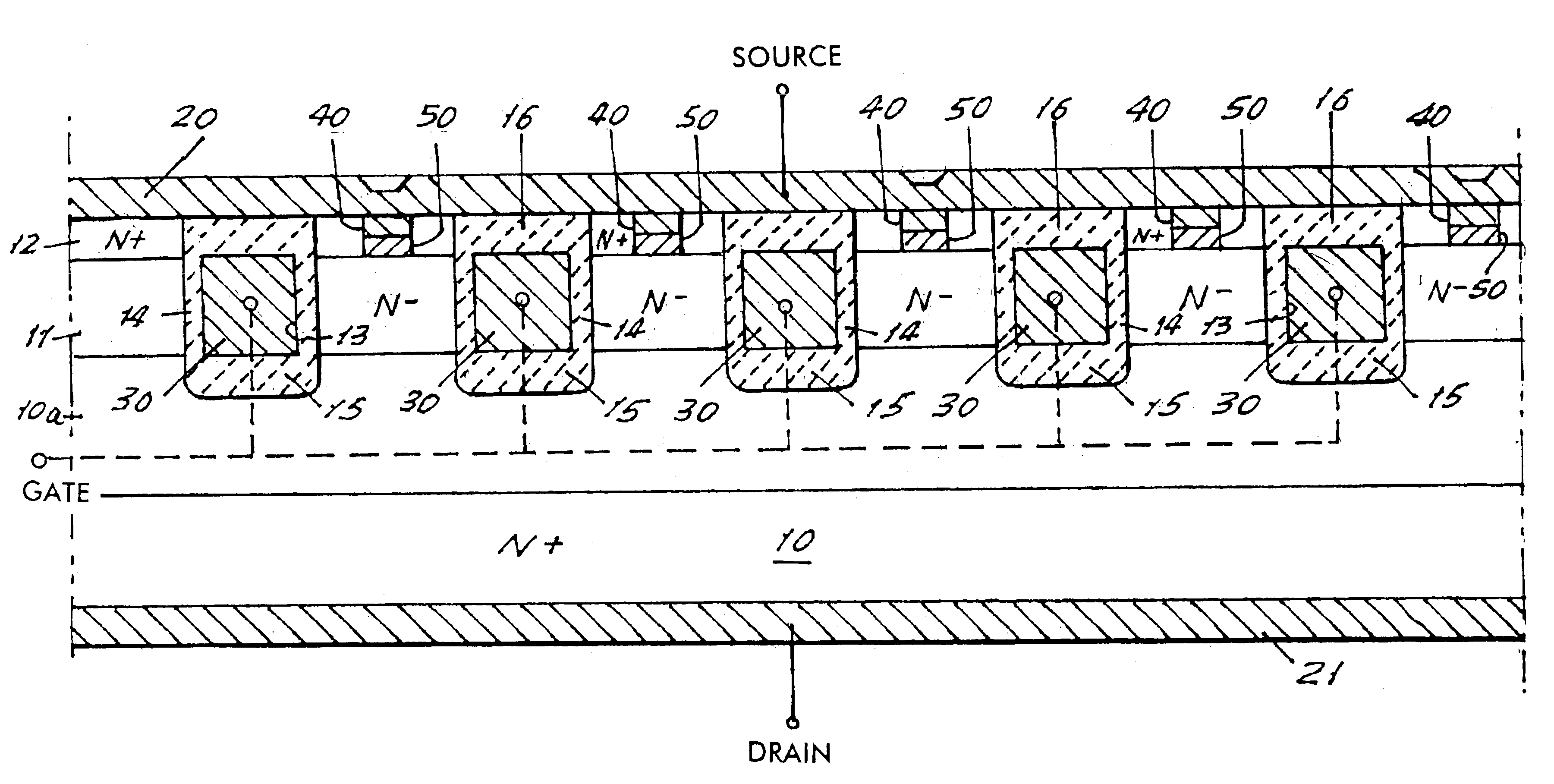
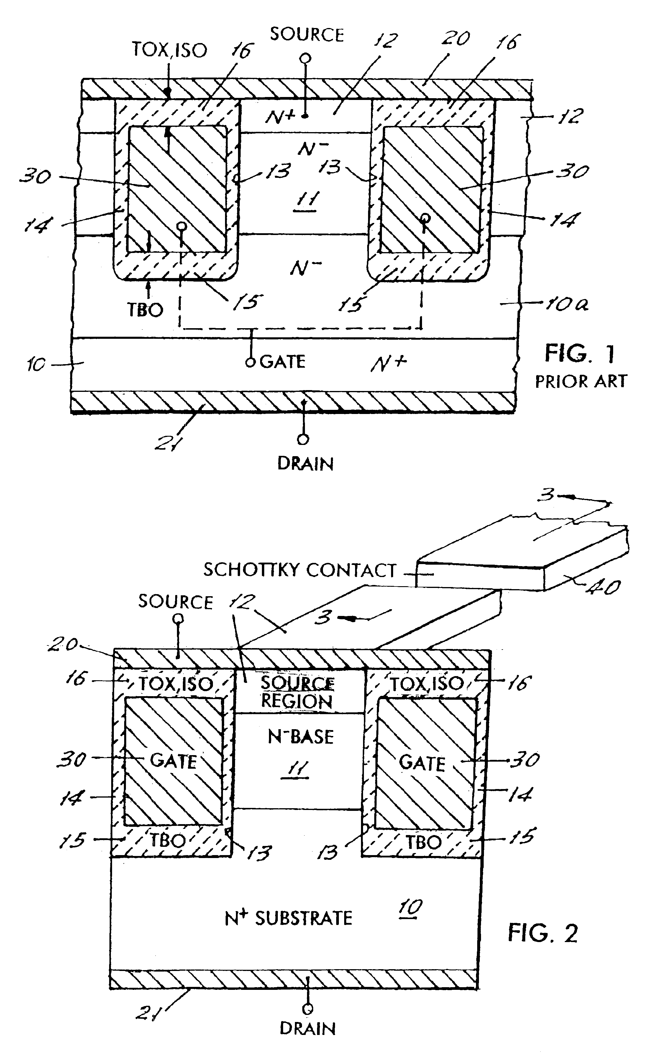
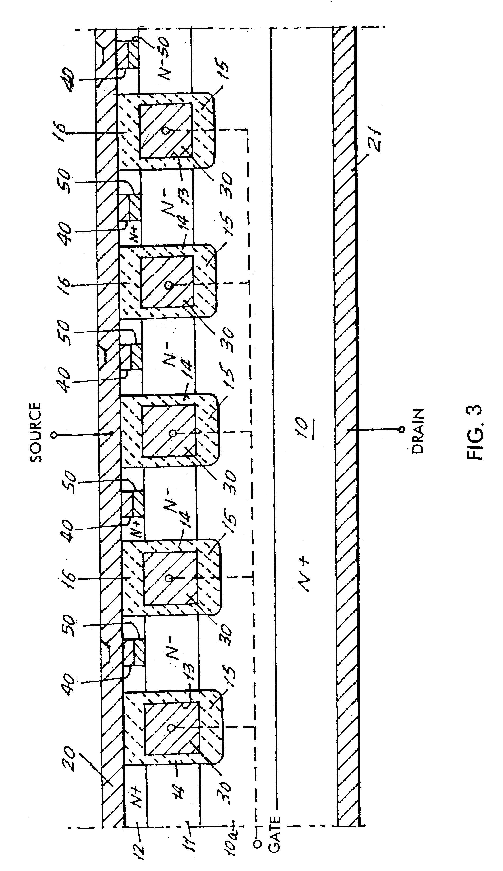
Referring first to FIGS. 2, 3, 4 and 5, the elements of those devices which are similar to those of FIG. 1 have the same identifying numeral.

In FIG. 2, the source region 12 has a laterally projecting region of any desired shape which contains spaced openings such as openings 40 (FIG. 3) of any desired shape through which the aluminum source contact 20 (or any other Schottky-forming metal) can project to contact base 11 and form a Schottky diode.

FIGS. 3 and 4 show the use of aluminum layers 50 as the Schottky forming barrier. Other Schottky barrier layer segments could be used. The opening 40 through the N+ layer 12 may have any desired geometry, and such openings may be distributed over at least a major portion of the area of the N+ source region 12 as shown in FIG. 3.

The modified structure of FIGS. 2, 3 and 4 achieves the following:

1. The source metal 20 on top of the N+ source region 12 adjacent cross-section makes ohmic contact to the N+ source region 12. However, a Schottky cont...


PUM


Abstract

A MOSgated device has spaced vertical trenches lined with a gate oxide and filled with a P type polysilicon gate. The gate oxide extends along a vertical N channel region disposed between an N+ source region and an N drift region. A Schottky barrier of aluminum is disposed adjacent the accumulation region extending along the trench to collect holes which are otherwise injected into the source region during voltage blocking. A common source or drain contact is connected to the N+ region and to the Schottky contact. A two gate embodiment is disclosed in which separately energized gates are connected to alternatively located gate polysilicon volumes.

Description

FIELD OF THE INVENTIONThis invention relates to semiconductor devices and more specifically to a trench type device with on conduction through an accumulated channel region.BACKGROUND OF THE INVENTIONVertical conduction devices in which on state conduction is through an accumulated channel region are well known. U.S. Pat. No. 6,580,123 dated Jun. 17, 2003 in the name of Naresh Thapar (IR-1799) and assigned to the assignee of the present invention shows such a device.FIG. 1 shows two adjacent cells of such a prior device in cross-section. The device of FIG. 1 comprises an N+ substrate 10 which has an N− epitaxially deposited drift region 10a and base region 11. A high concentration source region diffusion 12 is formed on the top of epitaxial region 11. The side walls of each of trenches 13 are lined with a gate oxide 14, a bottom oxide TBO 15, and top isolation oxide tox, iso 16. A top source contact 20 contacts N+ source region 12 and a bottom drain contact 21 contacts the bottom of...

Claims


Application Information

Patent Timeline
IPC IPC(8): H01L29/76H01L29/66H01L23/58H01L29/78
CPCH01L29/7828H01L29/7839H01L2924/0002H01L2924/00
Inventor THAPAR, NARESH
Owner INFINEON TECH AMERICAS CORP
Why Eureka
Try Eureka