Broadband variable gain amplifier with high linearity and variable gain characteristic

a variable gain amplifier and linearity technology, applied in amplifiers, amplifiers with semiconductor devices/discharge tubes, amplifiers, etc., can solve the problems of variable input impedance low noise figure of variable gain amplifiers, and achieve the effect of improving linearity and noise figur

Inactive Publication Date: 2005-04-19
INTEGRANT TECH
View PDF5 Cites 47 Cited by
  • Summary
  • Abstract
  • Description
  • Claims
  • Application Information

AI Technical Summary

Benefits of technology

[0012]Still another object of the present invention is to provide ...

Problems solved by technology

However, a noise figure of the variable gain amplifier is low owing to a parasitic capacitance of the transistor FET12.
Moreover,...

Method used


Image

  • Broadband variable gain amplifier with high linearity and variable gain characteristic
  • Broadband variable gain amplifier with high linearity and variable gain characteristic
  • Broadband variable gain amplifier with high linearity and variable gain characteristic

Examples


Embodiment Construction

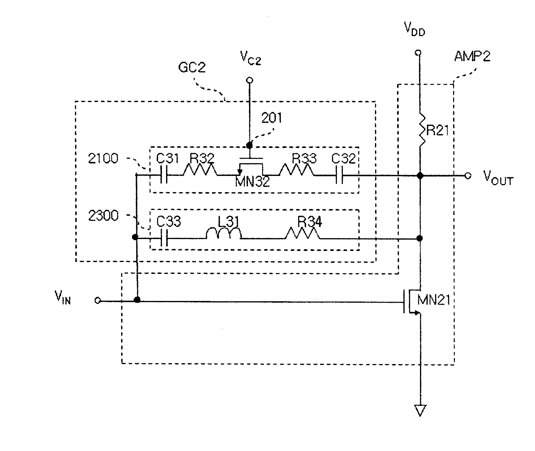
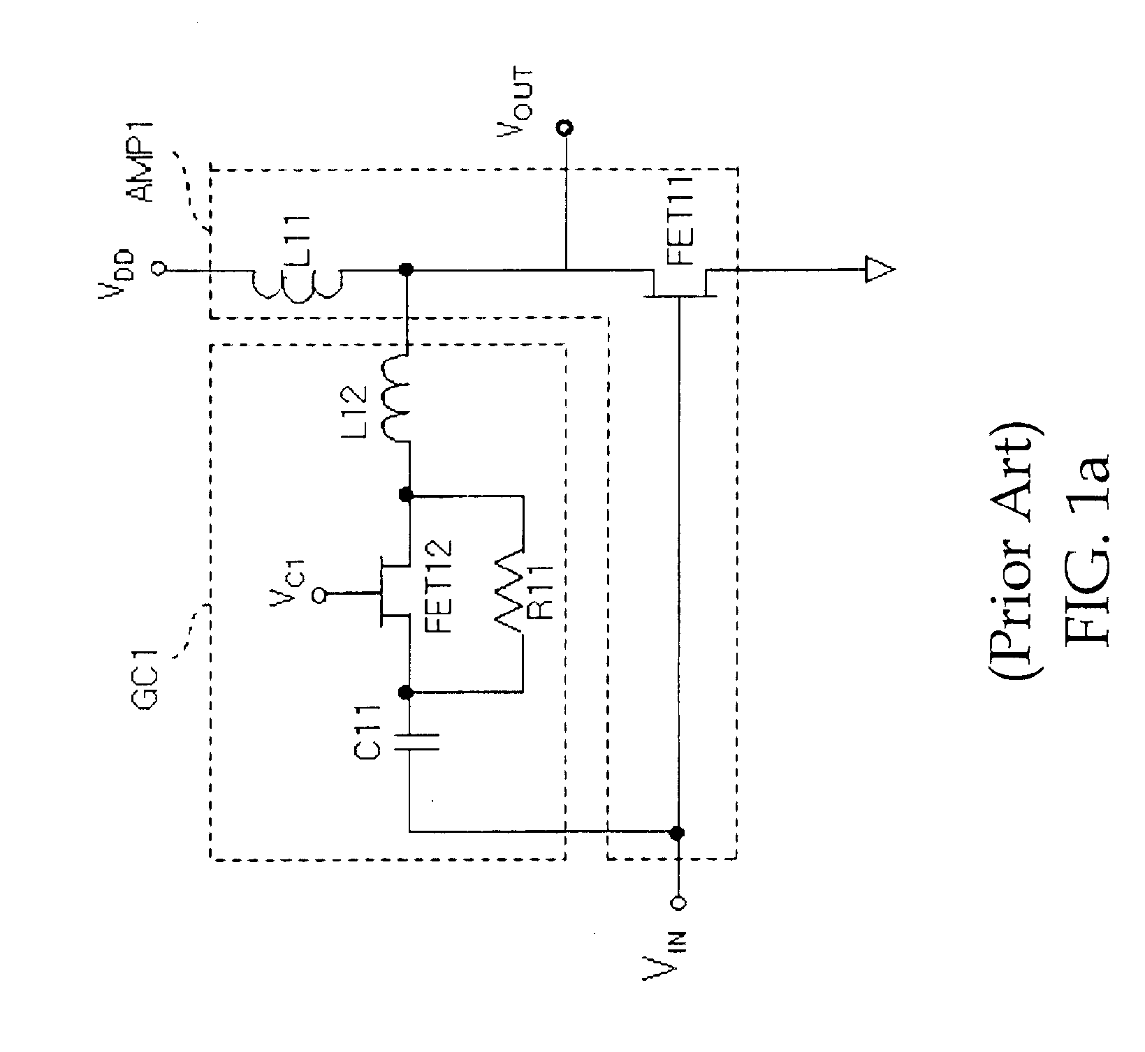
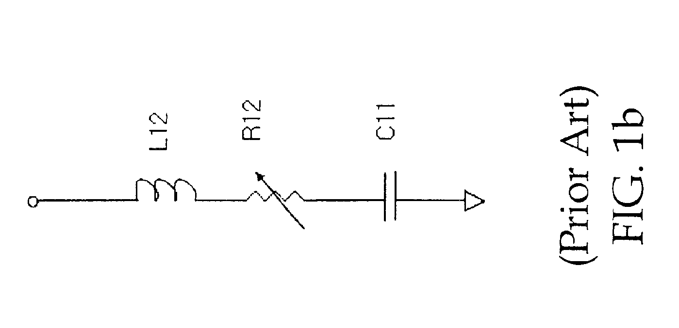
[0033]Hereinafter, preferred embodiments of the present invention will be described in detail with reference to the attached drawings.

[0034]The variable gain amplifier according to the present invention utilizes one or more active elements. Each active elements has a gate gn, source sn and drain dn. The active element has a characteristic that the direction and the quantity of current flowing from the drain dn to the source sn or vice versa are determined according to the polarity and the amount of the voltage applied to the gate gn and the source sn. Active elements having such characteristic includes bipolar junction transistor (BJT), junction field effect transistor (JFET), metal oxide semiconductor field effect transistor (MOSFET), and metal semiconductor field effect transistor (MESFET).

[0035]Some active elements have body terminal bn besides the gate gn, source sn, and drain dn. Such active elements have a characteristic that the direction and the quantity of current flowing f...


PUM


Abstract

A broadband variable gain amplifier with improved linearity and gain characteristic is provided. According to the present invention, the broadband variable gain amplifier comprises: an amplification unit for amplifying an input signal applied to an input terminal and outputting an amplified signal to an output terminal; and a gain control unit which is connected between the input and output terminals, and for controlling gain of said amplification unit, wherein said gain control unit comprises: a variable resistance unit whose resistance value is varied according to a control signal; and a broadband matching unit for proving an optimal impedance characteristic to the input terminal said amplification unit in a broad band, where in said variable gain resistance unit and said broadband matching unit is connected in parallel.

Description

TECHNICAL FIELD[0001]The present invention relates to a variable gain amplifier and, more particularly, a variable gain amplifier with high linearity and variable gain characteristic in a high frequency band.BACKGROUND OF THE INVENTION[0002]A variable gain amplifier is a device for maintaining a desired level of output signals by adjusting gain, in a radio frequency communication system.[0003]FIG. 1a shows a circuit diagram of a conventional feedback type variable gain amplifier disclosed in U.S. Pat. No. 6,285,257.[0004]The conventional feedback type variable gain amplifier disclosed in U.S. Pat. No. 6,285,257 is provided with an amplifier AMP1, and gain control circuit GC1 which is a feedback circuit coupled to the amplifier AMP1 and controls a value of the gain. The amplifier AMP1 includes a series-connected high frequency cutoff inductor L11 and amplifying field effect transistor FET11 across a power-supply potential terminal VDD and a ground potential terminal GND. The gate of ...

Claims


Application Information

Patent Timeline
IPC IPC(8): H03G1/00
CPCH03F1/342H03F3/45183H03G1/007H03F2200/108H03F2200/141H03F2203/45532H03F2200/117
Inventor CHO, YOUNGHOKIM, BO-EUNKIM, BONKEE
Owner INTEGRANT TECH
Why Eureka
Try Eureka