

Ceramic substrate for manufacture/inspection of semiconductor
a ceramic substrate and semiconductor technology, applied in the direction of turning machine accessories, natural mineral layered products, chucks, etc., can solve the problems of low fracture toughness value and easy cracking, and achieve the effect of high radian, reduced volume resistivity, and increased ability to absorb silicon wafers
- Summary
- Abstract
- Description
- Claims
- Application Information
AI Technical Summary
Benefits of technology
Problems solved by technology
Method used
Image

Examples
example 1
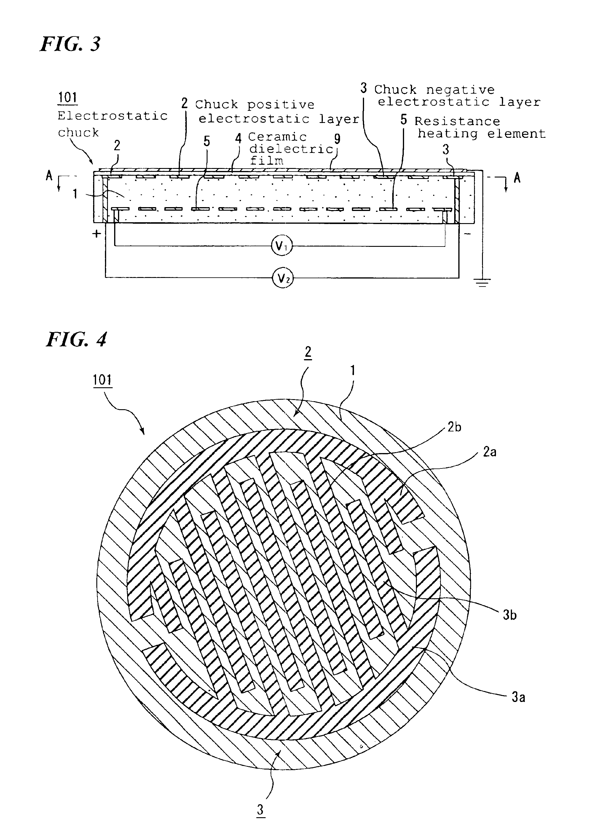
Production of Electrostatic Chuck (reference to FIG. 3)
[0202](1) Paste, which was obtained by mixing 1000 parts by weight of aluminum nitride powder (made by Tokuyama Corp., average particle diameter: 0.6 μm), 40 parts by weight of yttria (average particle diameter: 0.4 μm), 115 parts by weight of acrylic binder, 0.002 parts by weight of boron nitride, 5 parts by weight of dispersant and 530 parts by weigh of alcohol comprising 1-butanol and ethanol, was used to be formed by the doctor blade method so that a green sheet having a thickness of 0.47 mm was obtained.[0203](2) Next, after the green sheet was dried at 80° C. for 5 hours, portions which were to become through holes having diameters of 1.8 mm, 3.0 mm and 5.0 mm into which semiconductor wafer supporting pins are inserted, and portions which were to become conductor filled through holes for connecting external terminals were provided by punching.[0204](3) 100 parts by weight of tungsten carbide particles having an average par...
example 2
Production of an Electrostatic Chuck (reference to FIG. 5)
[0215](1) Paste, which was obtained by mixing 1000 parts by weight of aluminum nitride powder (made by Tokuyama Corp., average particle diameter: 0.6 μm), 40 parts by weight of yttria (average particle diameter: 0.4 μm), 115 parts by weight of acrylic binder, 0.002 parts by weight of boron nitride, 0.05 parts by weight of silica, 0.001 parts by weight of Na2O, 5 parts by weight of dispersant and 530 parts by weigh of alcohol comprising 1-butanol and ethanol, was used to be formed by the doctor blade method so that a green sheet having a thickness of 0.47 mm was obtained.[0216](2) Next, after the green sheet was dried at 80° C. for 5 hours, portions which were to become through holes having diameters of 1.8 mm, 3.0 mm and 5.0 mm into which semiconductor wafer supporting pins are inserted, and portions which were to become conductor filled through holes for connecting external terminals were provided by punching.[0217](3) 100 p...
example 3
Production of an Electrostatic Chuck 301 (FIG. 6)
[0233](1) Tungsten foil having a thickness of 10 μm was punched so that two electrodes having a shape shown in FIG. 9 were formed.
[0234]The two electrodes and tungsten wires as well as a mixture comprising 1000 parts by weight of aluminum nitride powder (made by Tokuyama Corp., average particle diameter: 0.6 μm), 40 parts by weight of yttria (average particle diameter: 0.4 μm), 115 parts by weight of acrylic binder, 0.002 parts by weight of boron nitride, 0.05 parts by weight of silica and 0.001 parts by weight of calcia, were put into a mold. Thereafter, they were hot-pressed at 1890° C. for 3 hours at a pressure of 200 kg / cm2 in nitrogen gas so that an aluminum nitride plate-shaped body having a thickness of 3 mm was obtained. This was cut out into a circular plate having a diameter of 230 mm so as to have a plate-shaped body. At this time, a thickness of the electrostatic electrode layer was 10 μm.[0235](2) This plate-shaped body i...
PUM
| Property | Measurement | Unit |
|---|---|---|
| Temperature | aaaaa | aaaaa |
| Thickness | aaaaa | aaaaa |
| Diameter | aaaaa | aaaaa |
Abstract
Description
Claims
Application Information