

Display module
- Summary
- Abstract
- Description
- Claims
- Application Information
AI Technical Summary
Benefits of technology
Problems solved by technology
Method used
Image

Examples
first embodiment
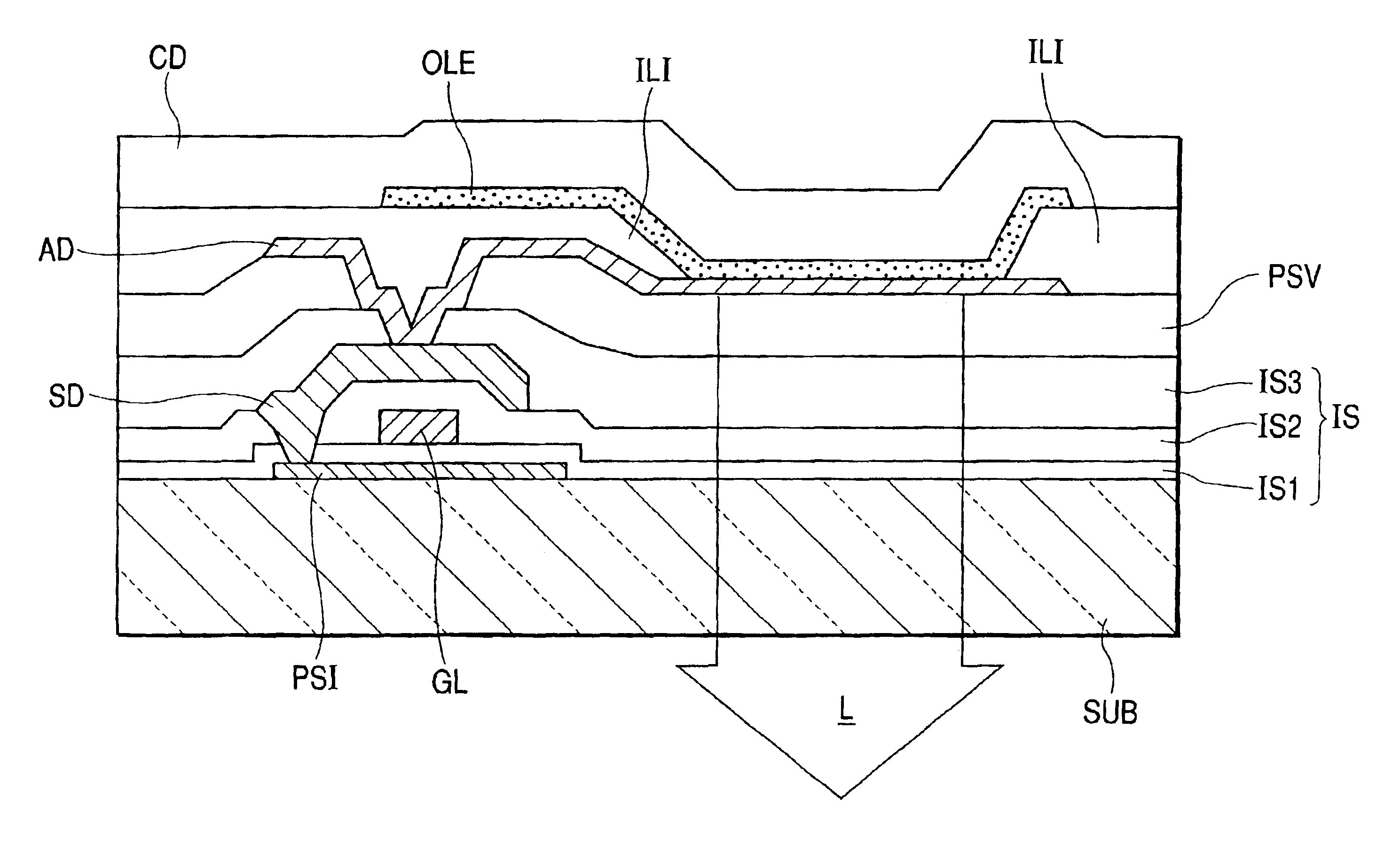
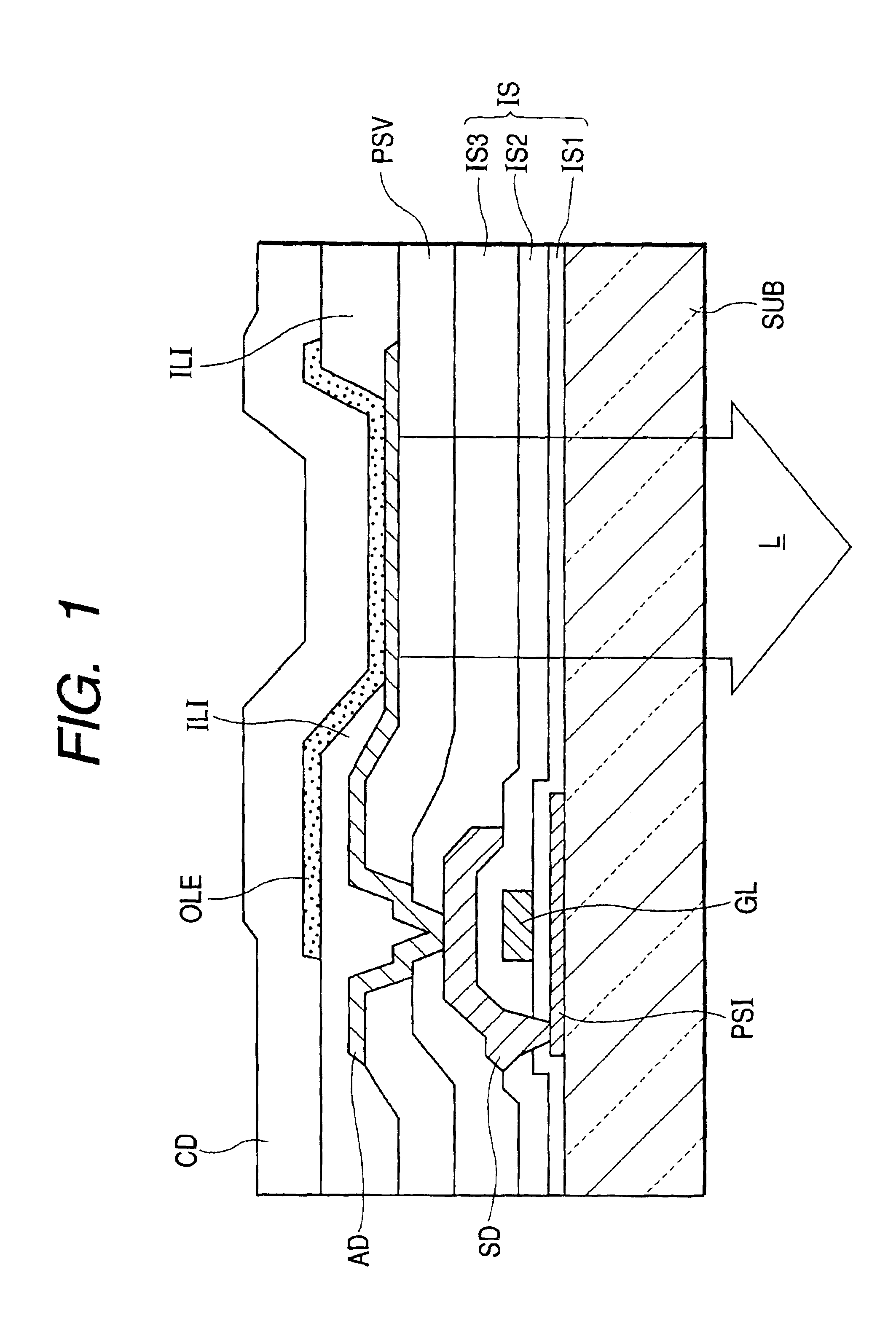
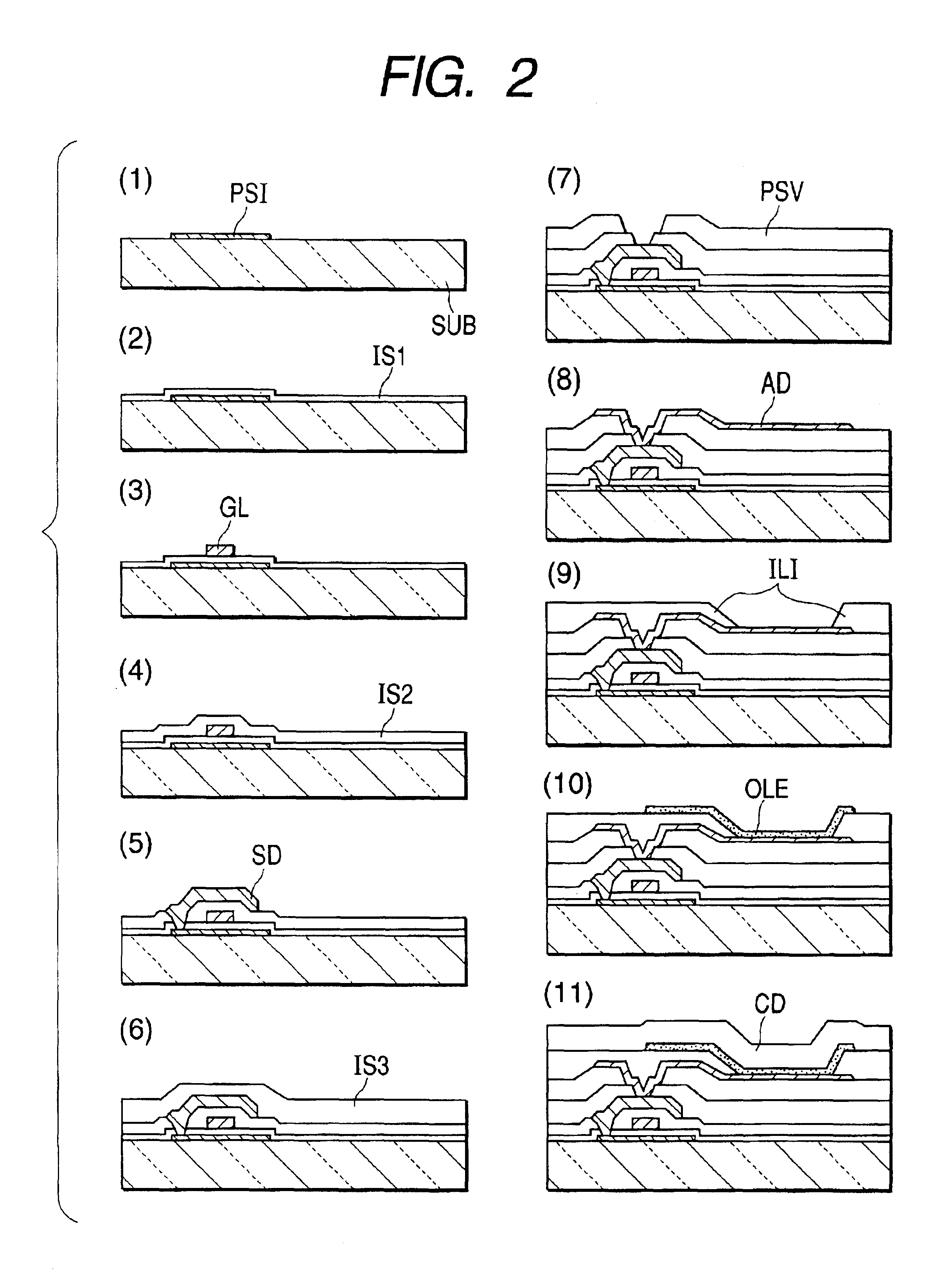
[0083]FIG. 2 is a typical drawing for describing a cross section near a pixel in the order of a production process in which an example of the production process of the display module of the first embodiment is described in the display module according to the present invention. This embodiment uses a thin film transistor of what is called the top gate structure, but also uses a thin film transistor of what is called the bottom gate structure in the same manner. This process is described below in the order of steps (1) to (11).
[0084](1) A polycrystalline silicon semiconductor layer PSI is patterned on a glass substrate SUB and laser annealing for crystallization is applied.
[0085](2) A first insulation layer IS1 is formed on it.
[0086](3) A gate line (scanning line) GL is formed by depositing and patterning a conductive thin film, such as titanium (Ti) or tungsten (W).
[0087](4) A second insulation layer IS2 is formed and a contact hole is perforated at a necessary place.
[0088](5) An alu...
fifth embodiment
[0111]FIG. 8 is a typical sectional view for describing the configuration of the circuit configuration of the display module according to the present invention. The same reference symbol as FIG. 1 corresponds to the same function part. This embodiment has the configuration in which the exit direction of light emission is set at the opposite side with a substrate. In the drawing, CD′ indicates a first electrode layer (cathode here) formed using a metal thin film and AD′ indicates a second electrode (anode here) formed using a transparent conductive film, such as ITO.
[0112]In this embodiment, the emission light in an organic light emitting layer OLE exits from the second electrode layer AD′. Accordingly, a sealing member that is not shown, but is provided on the side of the second electrode layer AD′ uses a transparent member, such as glass.
[0113]FIG. 9 is a top plan drawing near a pixel for describing an example of the circuit configuration of the display module according to the pres...
PUM
 Abstract
Description
Claims
Application Information