Wavelength-selective photonics device

a wavelength-selective, photonics technology, applied in the direction of lasers, semiconductor lasers, radiation controlled devices, etc., can solve the problems of limiting the wavelength range of the device, limiting the energy of the opto-electronic transition between bound states, and elusive efficient light emission prospects

Inactive Publication Date: 2005-05-10
QUANTUM SEMICON
View PDF4 Cites 74 Cited by
  • Summary
  • Abstract
  • Description
  • Claims
  • Application Information

AI Technical Summary

Benefits of technology

[0030]The wavelength selectivity, that is, the selectivity in photon-absorption or photon-emission by the active-layers, in accordance with photon energy, can be realized in different ways. Selecting and / or adjusting the parameters that control the wavelength selectivity of the active-layers in the stack, permits the implementation of devices operating in the visible spectrum, as well as in the infrared and ultra-violet, that suit a wide range of needs or applications.

Problems solved by technology

In spite of continued research efforts, efficient light emission has remained an elusive prospect for silicon devices and technologies, due to the indirect band-gap of silicon.
However, the band offsets are small compared to those of the III / V materials, thereby limiting the energy of the opto-electronic transitions between bound states, that is, limiting the range of wavelengths for device operation.

Method used


Image

  • Wavelength-selective photonics device
  • Wavelength-selective photonics device
  • Wavelength-selective photonics device

Examples


Embodiment Construction

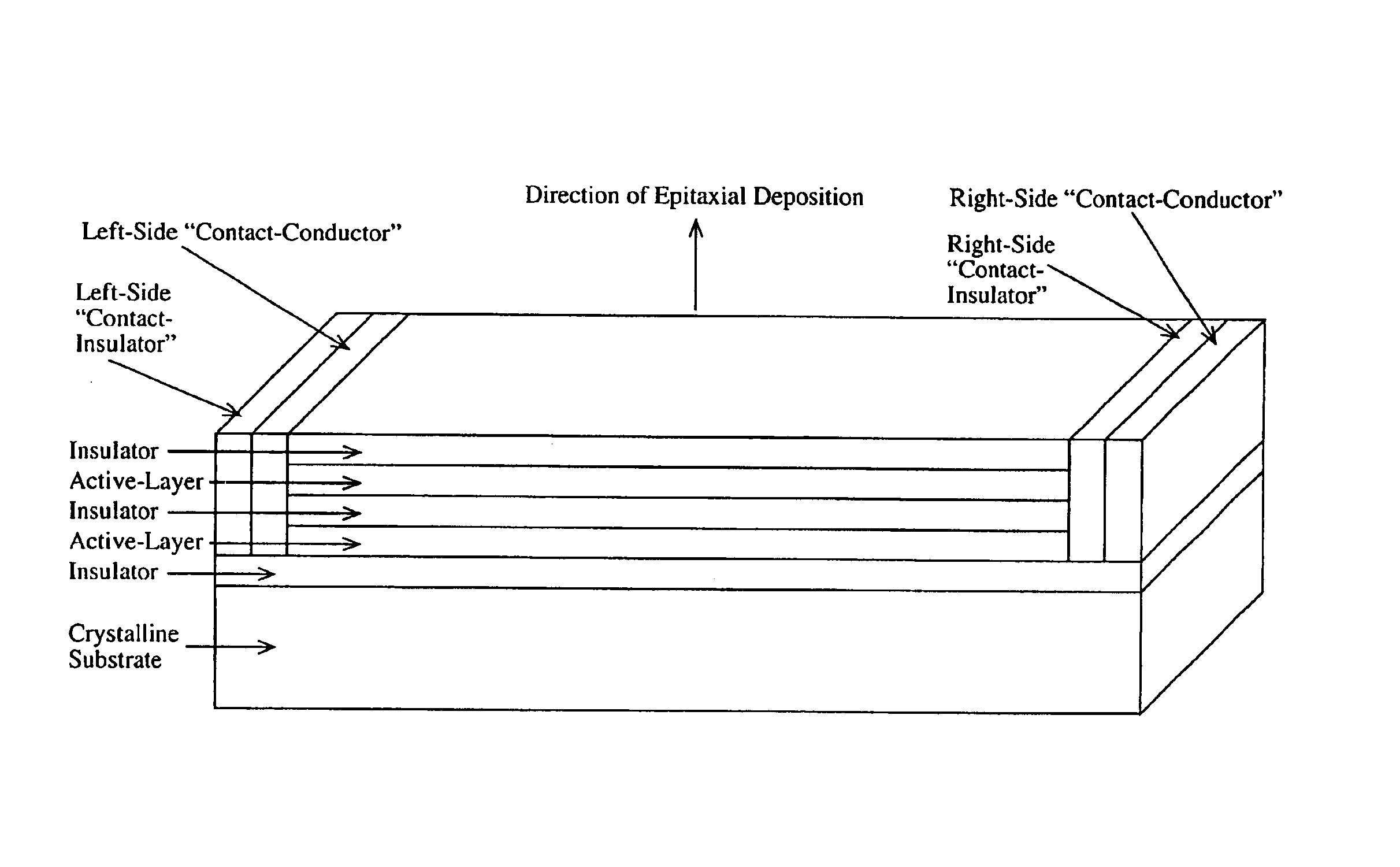
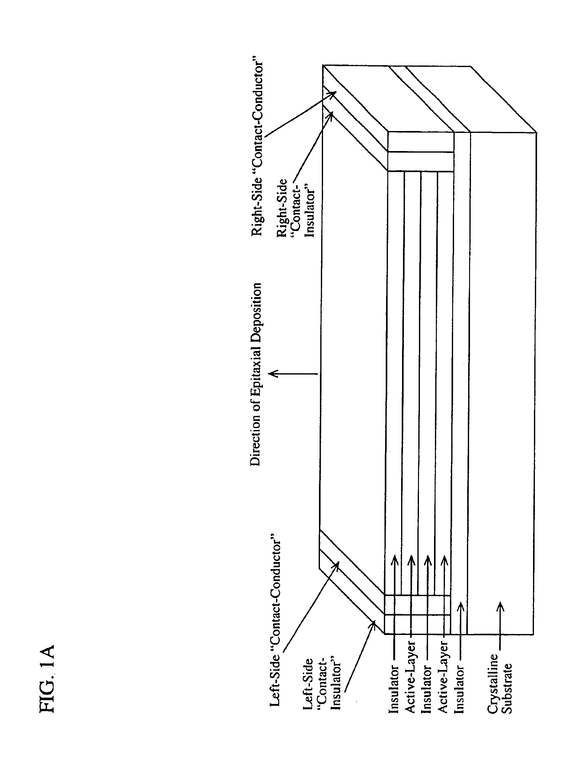
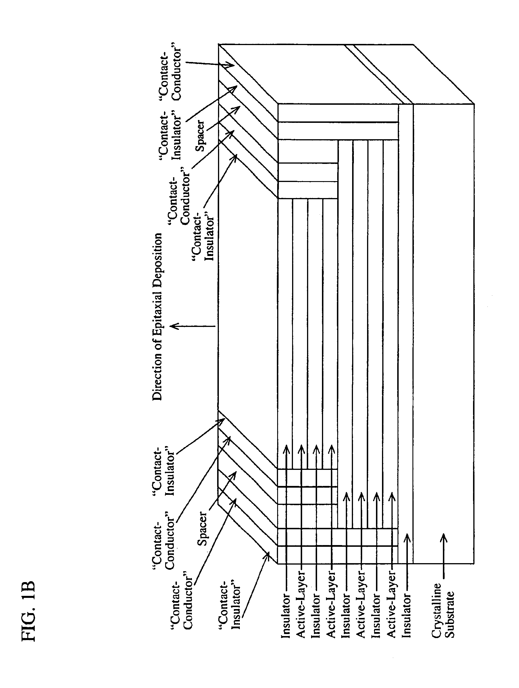
[0068]Advanced thin-film deposition techniques, such as Molecular Beam Epitaxy (MBE) and Atomic Layer Deposition (ALD) for example, enable the fabrication of very sophisticated doping and heterojunction profiles in the direction of epitaxial growth. Quantum Wells (QWs) require reduced dimensionality in one direction only, and for that reason are then easy to be made with such techniques. Quantum Wires and Quantum Dots require “reduced dimensionality” in two or three directions, respectively. Therefore, examples of quantized structures will, by default, mean Quantum Wells. However, this should not be seen as a conceptual limitation. If and when it becomes equally easy to fabricate Quantum Wires and Quantum Dots, the same concepts can (with suitable adaptations) also be used to implement these new device concepts, which can use and take advantage of quantization in more dimensions.

[0069]FIG. 1a shows a schematic of the device architecture according to the present invention. In FIG. 1b...


PUM


Abstract

A device comprising a number of different wavelength-selective active-layers arranged in a vertical stack, having band-alignment and work-function engineered lateral contacts to said active-layers, consisting of a contact-insulator and a conductor-insulator. Photons of different energies are selectively absorbed in or emitted by the active-layers. Contact means are arranged separately on the lateral sides of each layer or set of layers having the same parameters for extracting charge carriers generated in the photon-absorbing layers and/or injecting charge carriers into the photon-emitting layers. The device can be used for various applications: wavelength-selective multi-spectral solid-state displays, image-sensors, light-valves, light-emitters, etc. It can also be used for multiple-band gap solar-cells. The architecture of the device can be adapted to produce coherent light.

Description

[0001]The present application is a continuation-in-part of international application number PCT / EP00 / 05590 filed on Jun. 13, 2000, which claims the benefit of U.S. provisional patent application No. 60 / 140,671 filed on Jun. 14, 1999.FIELD OF THE INVENTION[0002]The present invention relates to the field of opto-electronic or photonic devices, including photon-absorption (or detection), suppression of photon-absorption, and photon-emission processesBACKGROUND OF THE INVENTION[0003]Historically, the preferred materials to implement opto-electronic or photonic devices have been materials with direct band-gaps. This fact is related to the significantly higher efficiency of such materials for light emission and / or absorption, for opto-electronic processes involving transitions across the band-gap.[0004]Silicon-based opto-electronic devices have consisted mainly of photo-detectors, such as Charge Coupled Devices (CCDs) and CMOS photo-gates or photo-diodes, for cost-sensitive products, and / ...

Claims


Application Information

Patent Timeline
Patent Type & Authority Patents(United States)
IPC IPC(8): H01L31/0264H01L31/0328H01L31/02H01L33/00H01S5/00H01L27/146H01L31/0216H01L31/028H01L31/0352H01L31/04H01L31/10H01L31/11H01L33/06H01L33/08
CPCB82Y20/00H01L27/14647H01L31/035236H01L31/11H01L27/14601H01L27/1462H01L27/14625H01L33/08H01L31/028H01L33/06H01L31/02162Y02E10/547
Inventor AUGUSTO, CARLOS J. R. P.
Owner QUANTUM SEMICON
Why Eureka
Try Eureka