Method to form selective cap layers on metal features with narrow spaces

a technology of metal features and selective cap layers, applied in the direction of liquid/solution decomposition chemical coatings, semiconductor/solid-state device details, coatings, etc., can solve the problems of insufficient thickness of cowp layers, and achieve the effects of reducing capacitive coupling, thermo-mechanical stress and thermal budget, and improving circuit performan

Inactive Publication Date: 2005-05-17
INFINEON TECH AG
View PDF13 Cites 40 Cited by
  • Summary
  • Abstract
  • Description
  • Claims
  • Application Information

AI Technical Summary

Benefits of technology

[0009]These and other problems are generally solved or circumvented, and technical advantages are generally achieve, by preferred embodiments of the present invention in which the conductive material is recessed prior to forming a barrier layer, eliminated the need for an additional cap layer. The above-mentioned problem, in which an insufficiently thick CoWP layer fails as a diffusion barrier to copper (Cu), necessitates the use of an additional cap layer. Embodiments of the present invention provide a method for eliminating the need for this additional cap layer and, thereby improve the overall circuit performance.
[0013]Embodiments of the present invention provide technical advantages by providing improved circuit performance, which is the result of a reduction in capacitive coupling, thermo-mechanical stress and thermal budget. The thermal budget reduction is the result of a decrease in the number of processing steps, which leads to lower processing costs. The reduction in capacitive coupling is the result of an elimination of the need for an additional dielectric cap layers (i.e. dielectric diffusion barriers) over the CoWP layer, such as SiN (Si3N4), SiC, SiCN or Blok™, as examples. The elimination of these additional dielectric cap layers also reduces the effective k-value of the dielectric stack in the interconnect architecture.

Problems solved by technology

The above-mentioned problem, in which an insufficiently thick CoWP layer fails as a diffusion barrier to copper (Cu), necessitates the use of an additional cap layer.

Method used


Image

  • Method to form selective cap layers on metal features with narrow spaces
  • Method to form selective cap layers on metal features with narrow spaces
  • Method to form selective cap layers on metal features with narrow spaces

Examples


Embodiment Construction

[0019]The making and using of the presently preferred embodiments are discussed in detail below. It should be appreciated, however, that the present invention provides many applicable inventive concepts that can be embodied in a wide variety of specific contexts. The specific embodiments discussed are merely illustrative of specific ways to make and use the invention, and do not limit the scope of the invention.

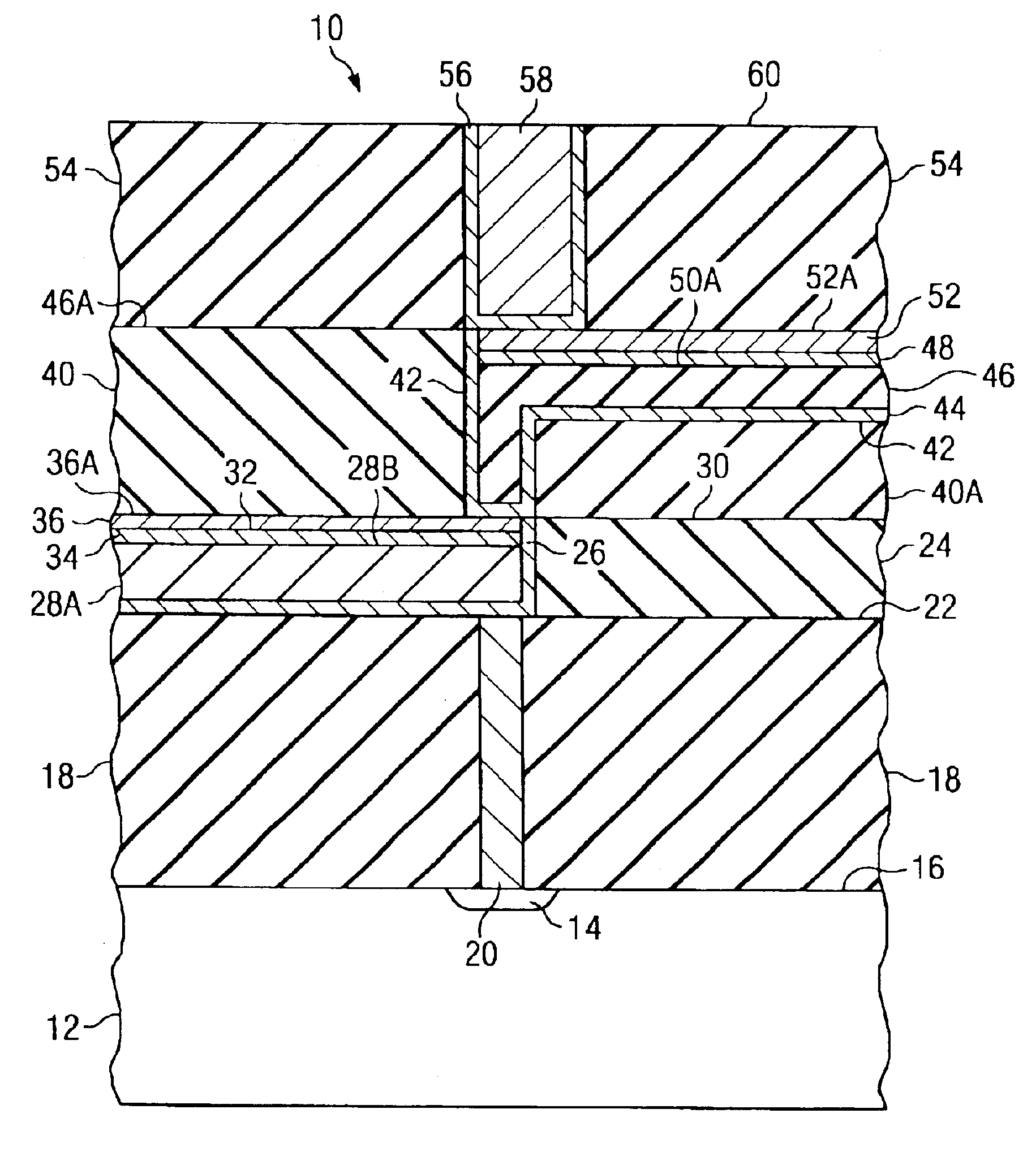
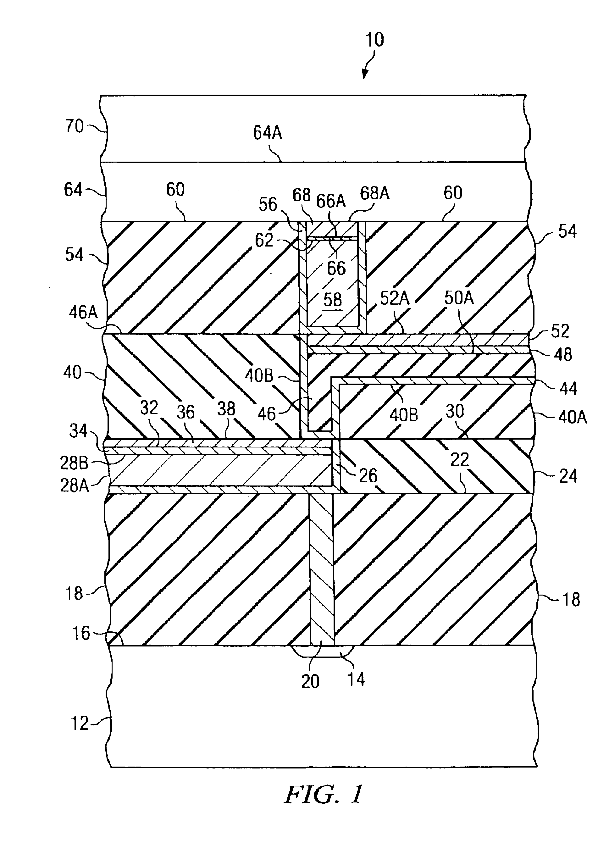
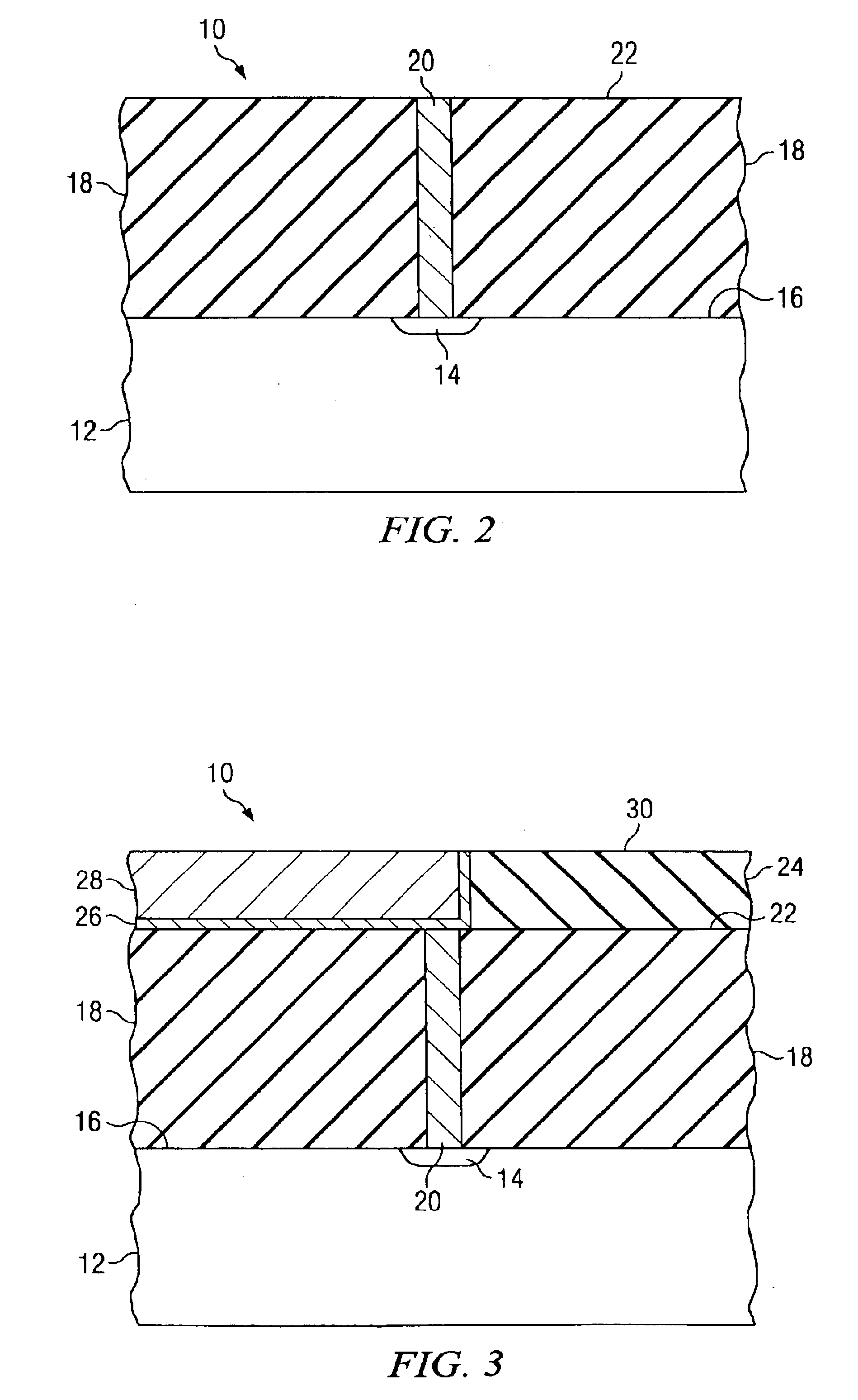
[0020]The present invention will be described with respect to preferred embodiments in a specific context, namely semiconductor devices having one or more metallization layers in which conductive lines are formed to form interconnects. Processes are described herein which bear on the elimination of an inorganic cap layer by recessing the surface of the copper conductors and vias to provide for a thicker, conducting diffusion barrier while still maintaining the overall thickness requirements for the metal / insulator stack. It is to be noted that the low-k dielectrics described ...


PUM

PropertyMeasurementUnit
dielectric constantaaaaaaaaaa
sizesaaaaaaaaaa
dielectric constantaaaaaaaaaa

Abstract

Interconnect layers on a semiconductor device containing logic circuits (microprocessors, Asics of others) or random access memory cells (DRAM's) are formed in a manner to significantly reduce the number of shorts between adjacent conductor / vias with narrow separations in technologies having feature sizes of 0.18 microns or smaller. This is accomplished by etching to form recessed copper top surfaces on each layer after a chemical-mechanical polishing process has been completed. The thickness of a selectively formed barrier layer on the recessed copper surfaces, is controlled to be essentially co-planar with the surrounding insulator surfaces. Because the barrier layers are recessed, shorting of adjacent conductive lines is prevented.

Description

TECHNICAL FIELD[0001]Embodiments of the present invention relate to integrated circuit devices using copper for interconnecting discrete circuit components as part of the processing of semiconductor devices, and more particularly, to modifications in semiconductor device processing resulting in a reduction of electrical shorts between metal lines and vias with high aspect ratios and narrow spaces.BACKGROUND[0002]As Ultra Large Scale Integration (ULSI) circuit density increases and device feature sizes approach 0.18 microns or less, increased numbers of patterned metal levels are required with decreasing spacing between metal lines at each level to effectively interconnect discrete semiconductor devices on the semiconductor chips. Typically, the different levels of metal interconnections are separated by layers of insulator material. These interposed insulating layers have etched holes filled with a conductive material, referred to as vias, which are used to connect one level of meta...

Claims


Application Information

Patent Timeline
Patent Type & Authority Patents(United States)
IPC IPC(8): C23C18/16H01L23/52H01L23/532H01L21/768
CPCH01L21/76849H01L21/76874H01L21/76877H01L23/53238H01L23/5329H01L2924/0002H01L2924/00
Inventor BARTH, HANS-JOACHIM
Owner INFINEON TECH AG
Why Eureka
Try Eureka