High-voltage semiconductor component

a high-voltage semiconductor and component technology, applied in the field of semiconductor devices, can solve problems such as stability not being maintained, and achieve the effect of high current load capacity and high “avalanche” ruggedness

Inactive Publication Date: 2005-05-17
INFINEON TECH AUSTRIA AG
View PDF81 Cites 17 Cited by
  • Summary
  • Abstract
  • Description
  • Claims
  • Application Information

AI Technical Summary

Benefits of technology

[0008]It is an object of the present invention to provide a robust semiconductor component of the kind initially mentioned, to be firstly distinguished by a high “avalanche” ruggedness and high current load capacity before and / or during breakdown and secondly simple to produce with reproducible properties in view of technological latitudes of fluctuation of manufacturing processes.

Problems solved by technology

U.S. Pat. No. 4,754,310 and U.S. Pat. No. 5,216,275) in which, however, specifically, improvements of the on-resistance RDS (on) but not of stability under current load, such as, in particular, robustness with regard to avalanche and short circuit in the high-current operation with high source-drain voltage, are sought.

Method used


Image

  • High-voltage semiconductor component
  • High-voltage semiconductor component
  • High-voltage semiconductor component

Examples


Embodiment Construction

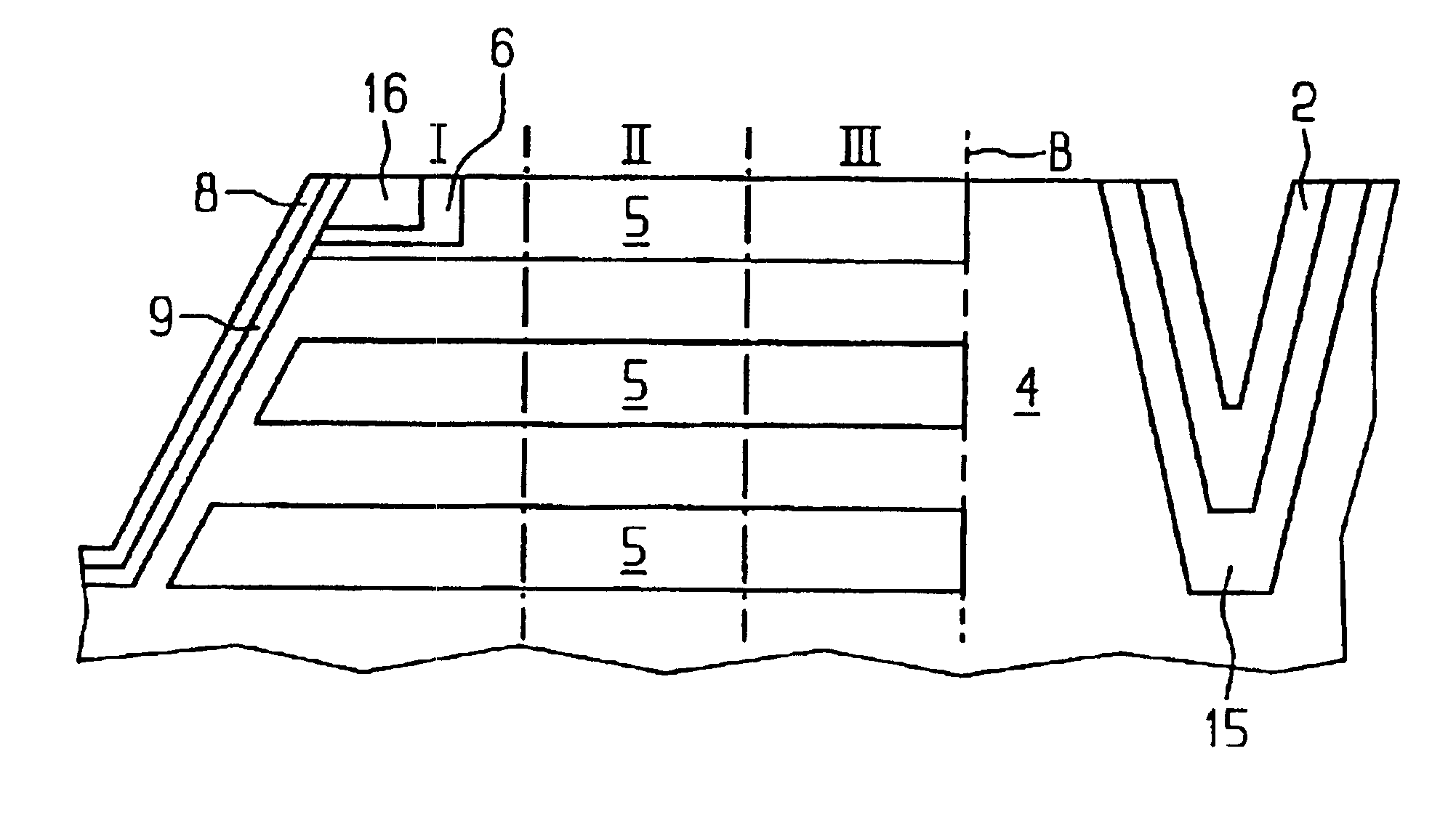
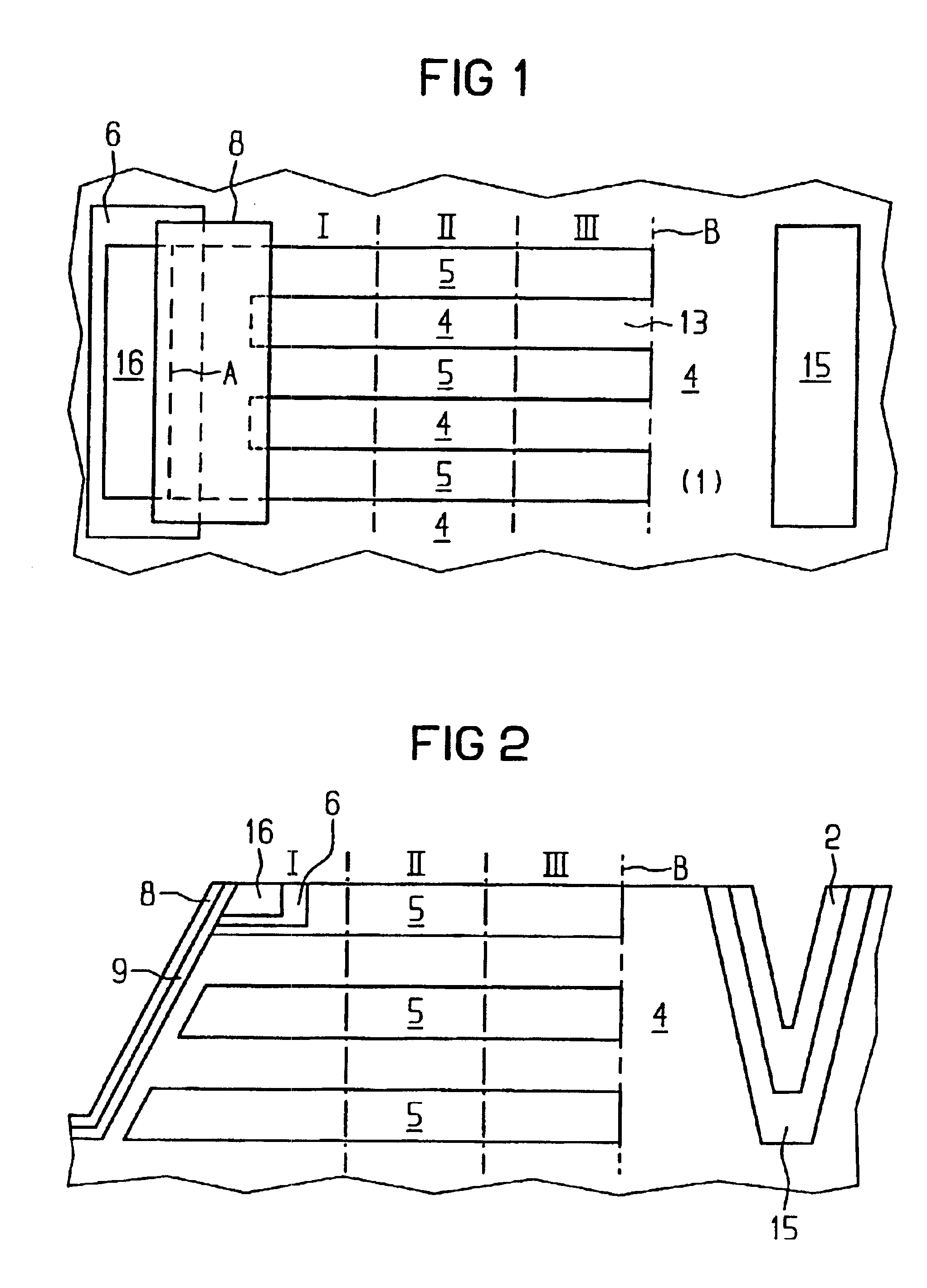
[0074]FIG. 1 depicts a top view of an n-channel MOS transistor with an n+-conductive drain zone 15, an n+-conductive source zone 16, a gate electrode 8, and a p-conductive area 5. This p-conductive area 5 extends finger-like into an n-conductive area 4 on a semiconductor substrate 1, such that the areas 4 and 5 are “nested” in each other. The gate electrode 8 may, for example, be made of polycrystalline silicon, whereas an isolation layer not shown in FIG. 1 below this gate electrode 8 is made, for example, of silicon dioxide and / or silicon nitride. In the p-conductive area 5, a p-charge excess is present in a zone I; a “neutral” charge, in a zone II; an n-charge excess, in a zone III. This means that in the area 5 in the zone I, the p-charge dominates the charge of the surrounding n-conductive area 5; that also in the zone II, the p-charge exactly compensates the charge of the surrounding n-conductive area 5; and that in the zone III, the p-charge is less than the charge of the sur...


PUM


Abstract

A semiconductor component has a semiconductor body comprising blocking pn junction, a source zone of a first conductivity type connected to a first electrode and bordering on a zone forming the blocking pn junction of a second conductivity type complementary to the first conductivity type, and a drain zone of the first conductivity type connected to a second electrode. The side of the zone of the second conductivity type facing the drain zone forms a first surface, and in the region between the first surface and a second surface located between the first surface and the drain zone, comprises areas of the first and second conductivity type nested in one another. The second surface coincides with the surface of the drain zone facing the source zone, such that the regions of the first and second conductivity type nested inside each other reach the drain zone.

Description

CROSS REFERENCE TO RELATED APPLICATION[0001]This application is a divisional of U.S. patent application Ser. No. 09 / 786,022 filed Nov. 9, 2001 Pat. No. 6,630,698, which is a 371 of PCT / DE99 / 01218 filed Apr. 22, 1999.TECHNICAL FIELD[0002]The present invention concerns a semiconductor device with a semiconductor body having a blocking pn-junction, a first zone of a first conductivity type, which is connected to a first electrode and abuts one of the zones of a second conductivity type opposite the first conductivity type forming the blocking pn-junction, and with a second zone of the first conductivity type, which is connected to a second electrode, whereby the side of the zone of the second conductivity type facing the second zone forms a first surface and in the region between the first surface and a second surface, which lies between the first surface and the second zone, areas of the first and of the second conductivity type are nested.BACKGROUND OF THE INVENTION[0003]Such semicon...

Claims


Application Information

Patent Timeline
Patent Type & Authority Patents(United States)
IPC IPC(8): H01L29/78H01L29/66H01L29/417H01L29/06H01L29/423H01L29/02H01L29/40H01L21/336
CPCH01L29/0634H01L29/7825H01L29/7801H01L29/7802H01L29/0696H01L29/1095H01L29/41766H01L29/4236H01L29/4238H01L29/4232H01L29/7811H01L29/7816H01L29/772
Inventor DEBOY, GERALDAHLERS, DIRKSTRACK, HELMUTRUEB, MICHAELWEBER, HANS MARTIN
Owner INFINEON TECH AUSTRIA AG
Why Eureka
Try Eureka