Fabrication of microstructures with vacuum-sealed cavity

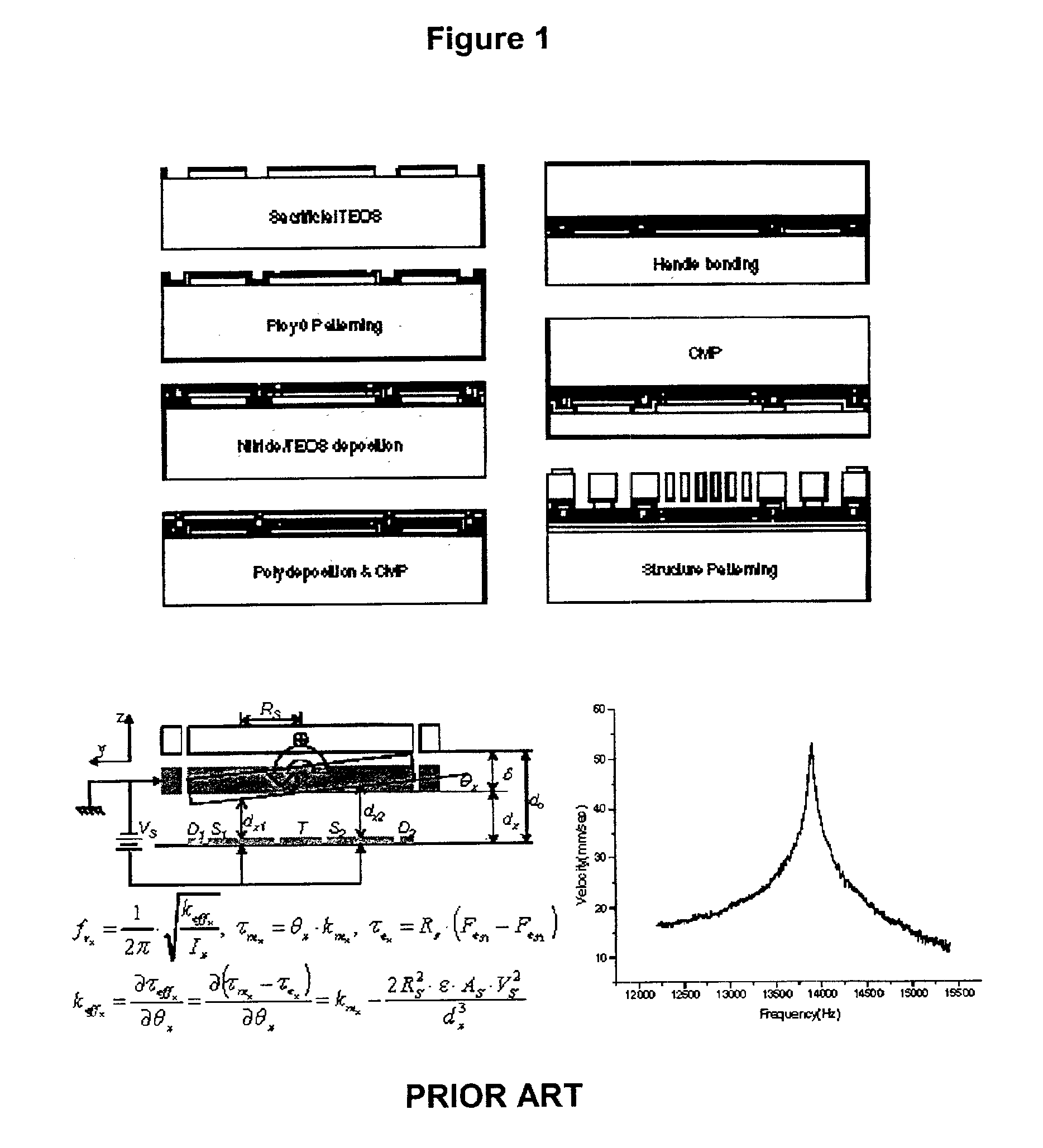
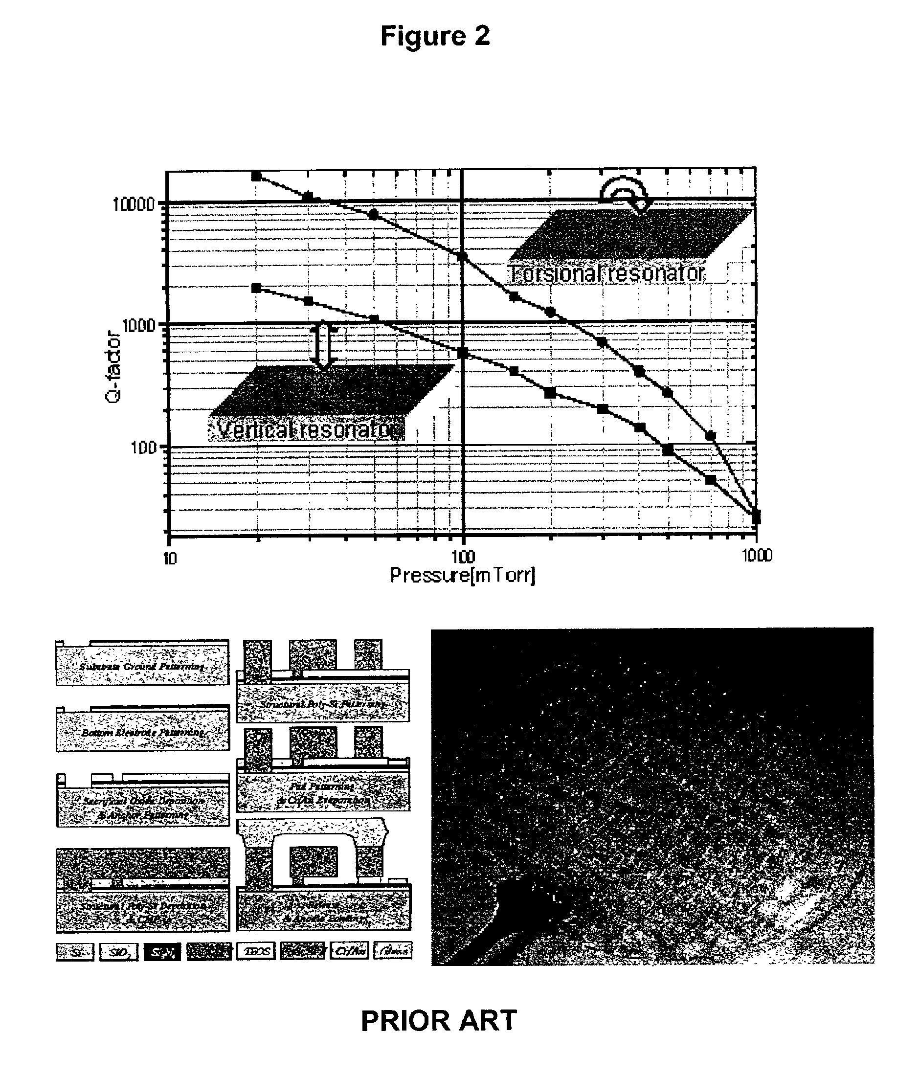
a vacuum sealing and microstructure technology, applied in the direction of acceleration measurement using interia forces, turn-sensitive devices, instruments, etc., can solve the problems of unsatisfactory glass frit bonding technique, unsatisfactory direct wafer bonding technique of two substrates, and little is known about this program. , to achieve the effect of long-term reliability

Inactive Publication Date: 2005-06-07
TELEDYNE DIGITAL IMAGING INC
View PDF17 Cites 51 Cited by
  • Summary
  • Abstract
  • Description
  • Claims
  • Application Information

AI Technical Summary

Benefits of technology

[0049]The present application relates to the use of an in-situ deposition of a tensile stress high Young's modulus material or combinations of materials after the deposition of the sealing aluminum alloy and before exposure to atmospheric pressure to achieve a reliable single-substrate wafer-level vacuum package capable of maintaining a vacuum-sealed cavity under vacuum condition around the moving and / or particular component of MEMS device. This vacuum environment can protect the moving or other component of a MEMS device against micro-contamination from the particles and slurry of the wafer dicing process, and against fluctuations of atmospheric conditions such as atmospheric pressure and relative humidity so as to ensure a long-term reliability for the moving or other component.

Problems solved by technology

It is known that Direct Wafer Bonding (DWB) of two substrates is not a suitable technique for vacuum packaged MEMS because of its required very high 1000° C. bonding temperature.
The Glass Frit Bonding technique discussed in some of the afore-mentioned Bosch Prior Art references is also unsatisfactory because its associated poor vacuum level degrades the Q-factor of most gyroscopes, accelerometers, RF switches and many other MEMS-based devices requiring packaging under a vacuum typically better than 1 Pa.
Unfortunately, the increased demand for higher yield and lower cost processes for the production of CMOS integrated MEMS devices in cost-sensitive markets, such as automotive and consumer electronics, requires the replacement of anodic bonding or other multiple substrates bonding techniques by a lower cost, single substrate, CMOS compatible wafer-level encapsulation technique.
Unfortunately, little is really known about this program.

Method used


Image

  • Fabrication of microstructures with vacuum-sealed cavity
  • Fabrication of microstructures with vacuum-sealed cavity
  • Fabrication of microstructures with vacuum-sealed cavity

Examples


Embodiment Construction

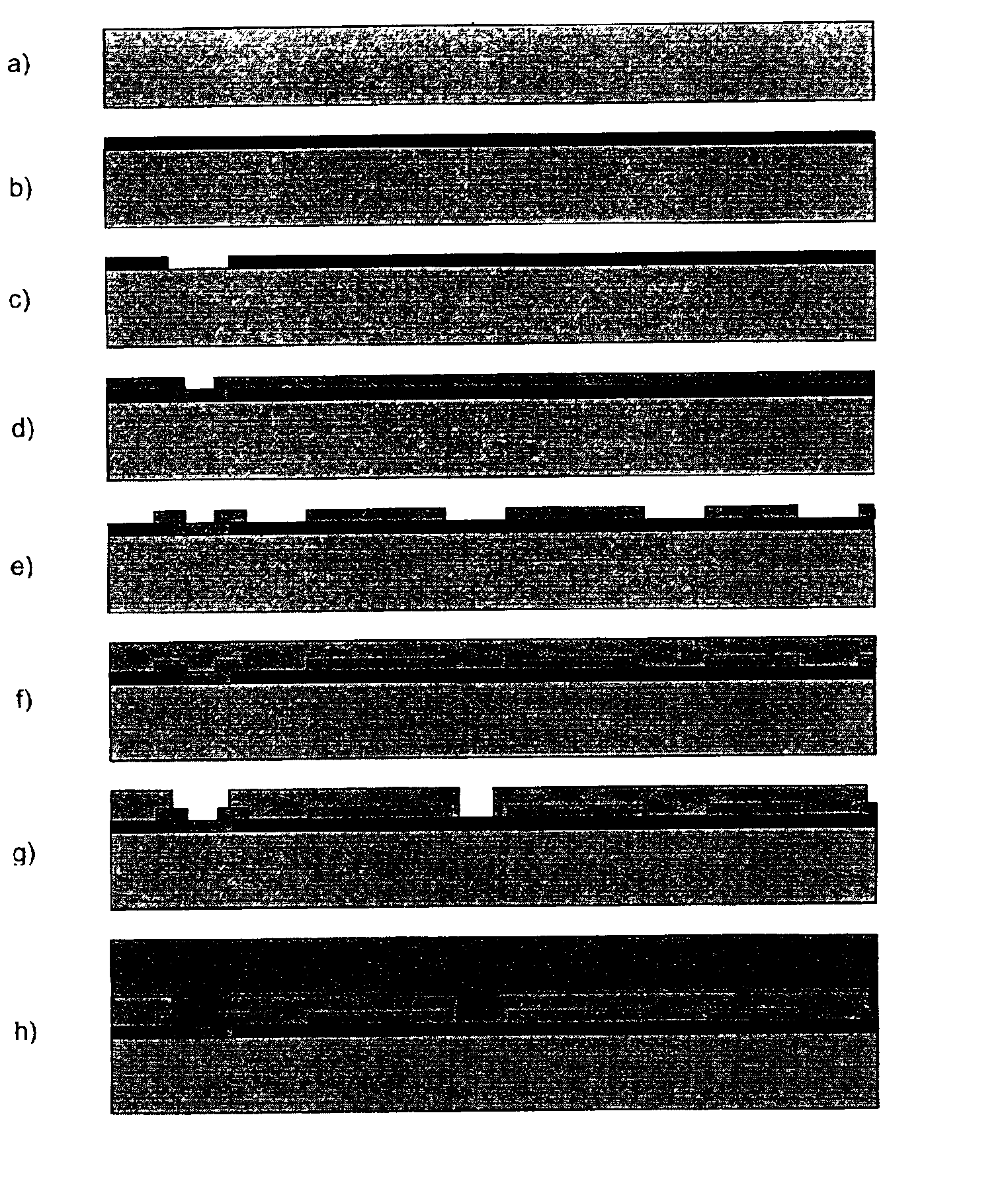
[0075]Reference will now be made to FIG. 8, which shows at steps (a) to (t), an integrated process for forming for a single-substrate, wafer-level protective cap as described in our co-pending U.S. patent application Ser. No. 10 / 120,528, filed Apr. 12, 2002, entitled ‘Wafer-level MEMS packaging’, the contents of which are herein incorporated by reference. In FIG. 8:[0076]step a) shows the silicon substrate;[0077]step b) shows the pad oxide growth;[0078]step c) shows the pad oxide patterning;[0079]step d) shows the surface polysilicon deposition;[0080]step e) shows the surface polysilicon patterning;[0081]step f) shows the deposition of the lower sacrificial material;[0082]step g) shows the patterning of the lower sacrificial material;[0083]step h) shows the structural isdp deposition and post-deposition doping;[0084]step i) shows the deposition and patterning of titanium nitride;[0085]step j) shows the photolithography and deep-etch of the Structural ISDP;[0086]step k) shows the dep...


PUM

PropertyMeasurementUnit
temperatureaaaaaaaaaa

Abstract

A cavity forming formed in an encapsulation structure under a vacuum in a vacuum chamber is sealed with a capping layer. A stiff protective layer under tensile stress is deposited on the capping layer prior to venting the vacuum chamber to atmospheric pressure. The capping layer is preferably aluminum or an aluminum alloy, and the protective layer is preferably δ-TiN having a suitable high Young's modulus.

Description

BACKGROUND OF THE INVENTION[0001]1. Field of the Invention[0002]This invention relates to the fabrication of microstructures, and in particular to the fabrication of microstructures with a vacuum-sealed cavity, for example containing a moving component, and further to the manufacture of Micro-Electro-Mechanical-Systems (MEMS), such as micro-gyroscopes, micro-accelerometers, resonant accelerometers, micro-mirrors, micro-motors, micro-actuators and other such micro-devices.[0003]2. Description of Related Art[0004]The integration of micro-devices with a moving component creates a very serious packaging challenge for several reasons. Some MEMS-based devices require the encapsulation to be done before dicing so that they are protected against micro-contamination from particles and dicing slurry while being processed like a standard semiconductor chip, without the need for dedicated equipment or processes for dicing, mounting and molding procedures inside the cleanrooms. Changes in atmosp...

Claims


Application Information

Patent Timeline
Patent Type & Authority Patents(United States)
IPC IPC(8): B22F1/00B81B7/00C23C14/06C23C14/00C23C14/32G01P15/08G01C19/56B22F1/0655G01C19/5719
CPCB22F1/0051B81C1/00325C23C14/0021G01P15/0802C23C14/228C23C14/325G01C19/5719C23C14/0641B81C2201/0167B22F1/0655
Inventor OUELLET, LUCANTAKI, ROBERTTREMBLAY, YVES
Owner TELEDYNE DIGITAL IMAGING INC
Why Eureka
Try Eureka