

Field emitter device comprising carbon nanotube having protective membrane
a field emitter and carbon nanotube technology, applied in the direction of discharge tube main electrodes, non-electron-emitting electrode materials, nanoinformatics, etc., can solve the problems of reducing affecting the efficiency and arcing of remaining plasma gas to damage the carbon nanotube, etc., to achieve the effect of reducing damage, prolonging the lifetime of the field emitter device, and facilitating electron emission
- Summary
- Abstract
- Description
- Claims
- Application Information
AI Technical Summary
Benefits of technology
Problems solved by technology
Method used
Image

Examples
Embodiment Construction
[0028]Embodiments of a field emitter device including carbon nanotubes having a protected membrane according to the present invention will be described in greater detail with reference to the appended drawings.
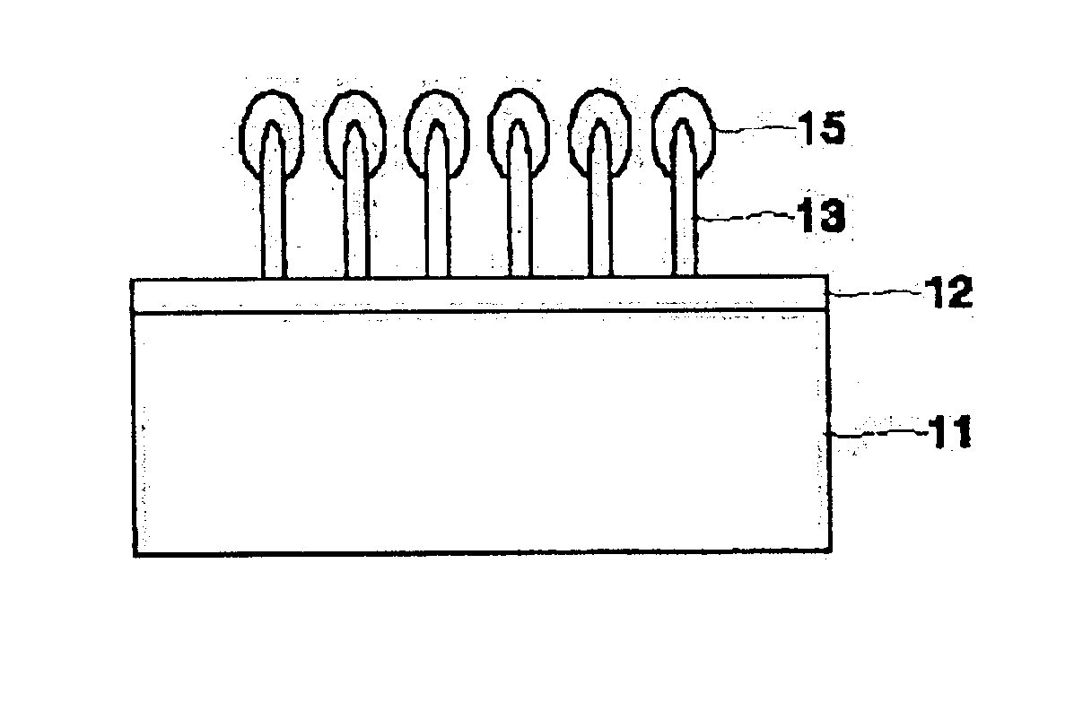
[0029]FIG. 3 shows the structure of a field emitter device according to an embodiment of the present invention. Referring to FIG. 3, the field emitter device includes a substrate 11, a cathode 12 stacked on the substrate 11, carbon nanotubes 13 on the cathode 12, and a protective membrane 15 coating each tip of the carbon nanotubes 13.
[0030]As a voltage is applied across the cathode 12 on one surface of the substrate 11 and an anode (not shown) formed on the surface of the substrate 11 opposite to opposite to the cathode 12, and the generated electric energy is greater than the work function of electrons, electrons are emitted from the tips of the carbon nanotubes 13.
[0031]Since the carbon nanotubes 13 inherently have a weak working field strength, an electron emission (diode ...
PUM
| Property | Measurement | Unit |
|---|---|---|
| temperature | aaaaa | aaaaa |
| current emission | aaaaa | aaaaa |
| pressure | aaaaa | aaaaa |
Abstract
Description
Claims
Application Information