Multilayer ceramic electronic component and mounting structure and method for the same

a technology of electronic components and mounting structures, applied in the direction of fixed capacitor details, printed circuit non-printed electric components association, final product manufacture, etc., can solve the problems of reduced voltage resistance, failure to mount, inferior wettability of solder alloys, etc., and achieve high voltage resistance

Active Publication Date: 2005-06-07
MURATA MFG CO LTD
View PDF3 Cites 52 Cited by
  • Summary
  • Abstract
  • Description
  • Claims
  • Application Information

AI Technical Summary

Benefits of technology

[0009]In order to overcome the problems described above, preferred embodiments of the present invention provide a mounting structure for providing a multilayer ceramic electronic component having high voltage resistance, a mounting method for constructing such a mounting structure, and a multilayer ceramic electronic component that has outstanding solderability and can be used in the mounting method.
[0014]The above-described mounting structure prevents surface leakage during the application of high voltage. The thermoplastic resin layer, covering substantially the entire surface except for the soldered portion of the multilayer ceramic electronic component and a portion of the solder, prevents dense potential distributions at the edges of the external electrodes and at a dielectric ceramic surface between the external electrodes. That is, the thermoplastic resin layer reduces the concentration of the electrical field to prevent surface leakage. This structure, therefore, provides high voltage resistance.
[0017]This thermoplastic resin layer, having a thickness of about 1.0 to about 50 μm, effectively prevents oxidation of the external electrodes and is readily molten by heat for the soldering to cover a portion of the solder.
[0018]According to another preferred embodiment of the present invention, the entire surface of the multilayer ceramic electronic component is covered with the thermoplastic resin layer. This thermoplastic resin layer also maintains the cleanliness of the external electrodes to provide outstanding wettability of the solder used, which ensures outstanding solderability even when using lead-free solders, as described above. This thermoplastic resin layer, therefore, prevents solder defects, and thus, enables efficient mounting.
[0019]Furthermore, during the mounting, the electronic component is soldered to the substrate while the thermoplastic resin layer is molten to flow. After the mounting, the thermoplastic resin layer covers substantially the entire surface except for the soldered portion of the electronic component. The thermoplastic resin layer, therefore, prevents surface leakage across the external electrodes to ensure high voltage resistance.

Problems solved by technology

If, therefore, high voltage is applied on the monolithic ceramic capacitor 1, surface leakage (discharge across the external electrodes 4) readily occurs, which reduces the voltage resistance.
These solder alloys, however, have inferior wettability than conventional Sn—Pb alloys.
Therefore, if the surfaces of the external electrodes 4 are oxidized, the use of these solder alloys may lead to unsuccessful mounting.

Method used


Image

  • Multilayer ceramic electronic component and mounting structure and method for the same
  • Multilayer ceramic electronic component and mounting structure and method for the same
  • Multilayer ceramic electronic component and mounting structure and method for the same

Examples


example

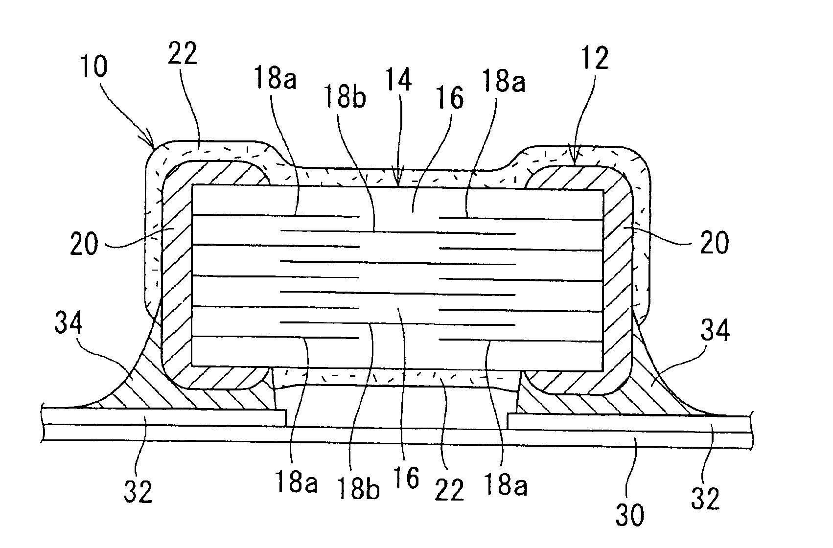
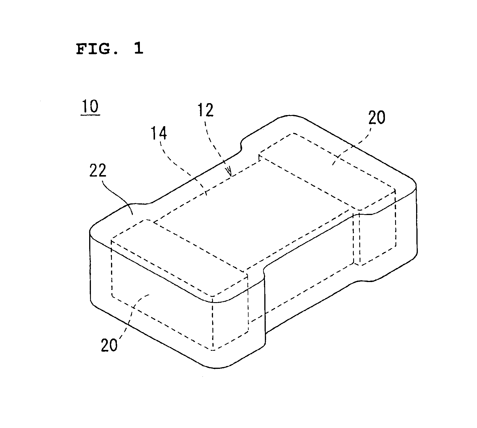
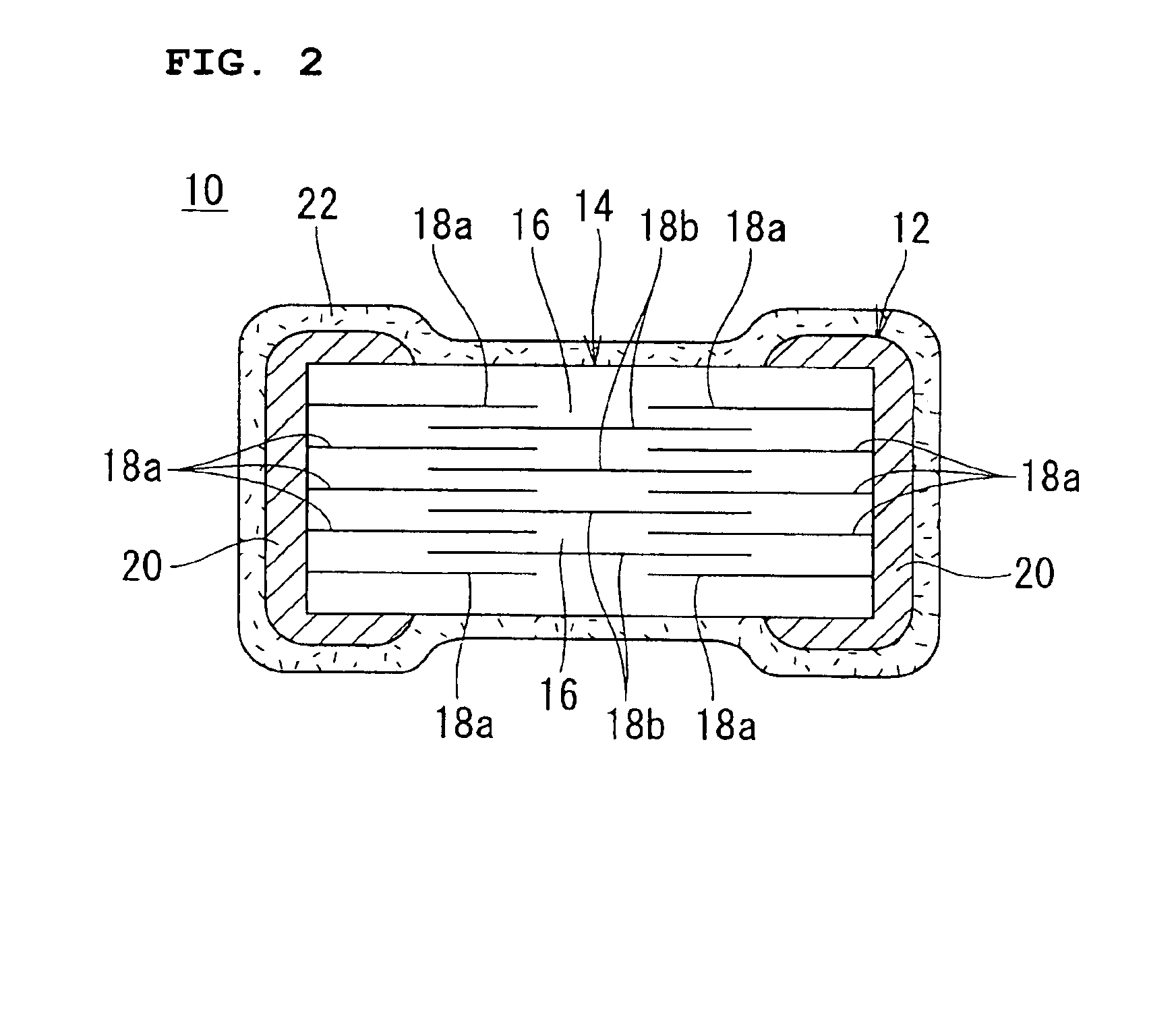
[0047]Monolithic ceramic capacitors were produced as an example of multilayer ceramic electronic components according to various preferred embodiments of the present invention. First, a ceramic slurry was prepared from a dielectric ceramic material. This slurry was shaped with PET films to form ceramic green sheets having a thickness of about 20.0 μm. Then, internal electrode patterns that provide thousands of chips for each printed area were printed on the ceramic green sheets with a nickel paste. The amount of the paste applied was adjusted such that the electrode thickness after firing was about 1.0 μm.

[0048]These ceramic green sheets were dried. Then, a predetermined number of the sheets were laminated, pressed under predetermined conditions, and cut to a predetermined size to form green chips, where the target capacitance was 1,000 pF. These green chips were fired at a predetermined temperature to prepare base composites of ceramic layers and internal electrodes. Subsequently, ...


PUM

PropertyMeasurementUnit
thicknessaaaaaaaaaa
temperatureaaaaaaaaaa
melting pointaaaaaaaaaa

Abstract

A multilayer ceramic electronic component is prepared by covering a capacitor element with a thermoplastic resin layer that is mounted on a substrate by soldering. The thermoplastic resin layer is molten due to the heat required for soldering. The molten resin layer flows to expose external electrodes of the electronic component. The exposed external electrodes are soldered to electrodes of the substrate. In the resultant mounting structure, the thermoplastic resin layer covers substantially the entire surface except for the soldered portion of the electronic component and a portion of the solder.

Description

BACKGROUND OF THE INVENTION[0001]1. Field of the Invention[0002]The present invention relates to multilayer ceramic electronic components and mounting structures and methods for the electronic components. In particular, the present invention relates to a multilayer ceramic electronic component, such as a monolithic ceramic capacitor, a structure in which the electronic component is mounted on a substrate by soldering, and a method for mounting the electronic component on the substrate by soldering.[0003]2. Description of the Related Art[0004]A monolithic ceramic capacitor is an example of multilayer ceramic electronic components. Referring to FIG. 5, a monolithic ceramic capacitor 1 includes a base composite of ceramic layers 2 and internal electrodes 3. The internal electrodes 3 are arranged across the thickness of the base composite, are alternately led to either end surface of the base composite, and are connected to external electrodes 4 disposed at both end surfaces of the base...

Claims


Application Information

Patent Timeline
Patent Type & Authority Patents(United States)
IPC IPC(8): H05K3/34H01G4/12H01G2/10H01G4/224H05K1/18
CPCH01G2/103H05K3/3442H05K2201/0129Y10T29/43H05K2201/10977Y10T29/435H05K2201/10636Y02P70/50H01G4/12
Inventor KAYATANI, TAKAYUKIKOBAYASHI, SHINICHI
Owner MURATA MFG CO LTD
Why Eureka
Try Eureka