Thin film transistor with plural channels and corresponding plural overlapping electrodes

Inactive Publication Date: 2005-06-14
SEMICON ENERGY LAB CO LTD
View PDF20 Cites 62 Cited by
  • Summary
  • Abstract
  • Description
  • Claims
  • Application Information

AI Technical Summary

Benefits of technology

[0085]In the case that the first electrode 11 and the second electrodes 15 are electrically connected, the electric field effect mobility and the sub-threshold coefficient can be made smaller and the on-state current can be made larger as the dielectric constant of the first insulating film 12 is closer to that of the second insulating film 14.
[0086]As the film thickness of the first insulating film 12 in the area where the first electrode 11 overlaps with the channel-formed regions 18a and 18b is closer to that of the second insulating film 14 in the area where the second electrodes 15a and 15b overlap with the channel-formed regions 18a and 18b, the electric field effect mobility and the sub-threshold coefficient can be made smaller and the on-state current can be made larger when each of the above-mentioned two film thicknesses is uniform. When the film thickness of the first insulating film in the area where it overlaps with the first electrode 11 is represented by d1 and the film thickness of the second insulating film in the area where it overlaps with the second electrodes 15 is represented by d2, it is desirable that d1 and d2 satisfy the following: |d1−d2|/d1≦0.1 and |d1−d2|/d2≦0.1. It is more desirable that d1 and d2 satisfy the following: |d1−d2|/d1≦0.05 and |d1−d2|/d2≦0.05.
[0087]It is most preferable that in the state that the first electrode 11 is not electrically connected to the second electrodes 15a and 15b, the threshold value of the thin film transistor when ground voltage is applied to the first electrode 11 is made substantially equal to the threshold value of the thin film transistor when ground voltage is applied to the second electrodes 15 and

Problems solved by technology

However, TFTs have low electric field effect mobility and cannot operate by frequencies necessary for processing picture signals.
However, as the density of pixels becomes larger, the pitch of the pixels becomes narrower; therefore, it is considered that the system in which a driver IC is mounted has a limit.
An increase in the number of the connecting terminals causes an increase in the probability that contact faults are generated.
As a result, it is unsuccessful that a semiconductor device using this as a display is made small-sized, and the

Method used


Image

  • Thin film transistor with plural channels and corresponding plural overlapping electrodes
  • Thin film transistor with plural channels and corresponding plural overlapping electrodes
  • Thin film transistor with plural channels and corresponding plural overlapping electrodes

Examples


example 1

[0108]Manufacturing steps of manufacturing a semiconductor device according to the present invention will be described. In this example, a method of simultaneously manufacturing a pixel section and TFT's (n-channel type TFT's and p-channel type TFT's) for a driving circuit provided near the pixel section, on the same substrate will be described in detail. In this example, an example in which the first structure TFT is formed as a switching element and common voltage is applied to the one-side electrodes.

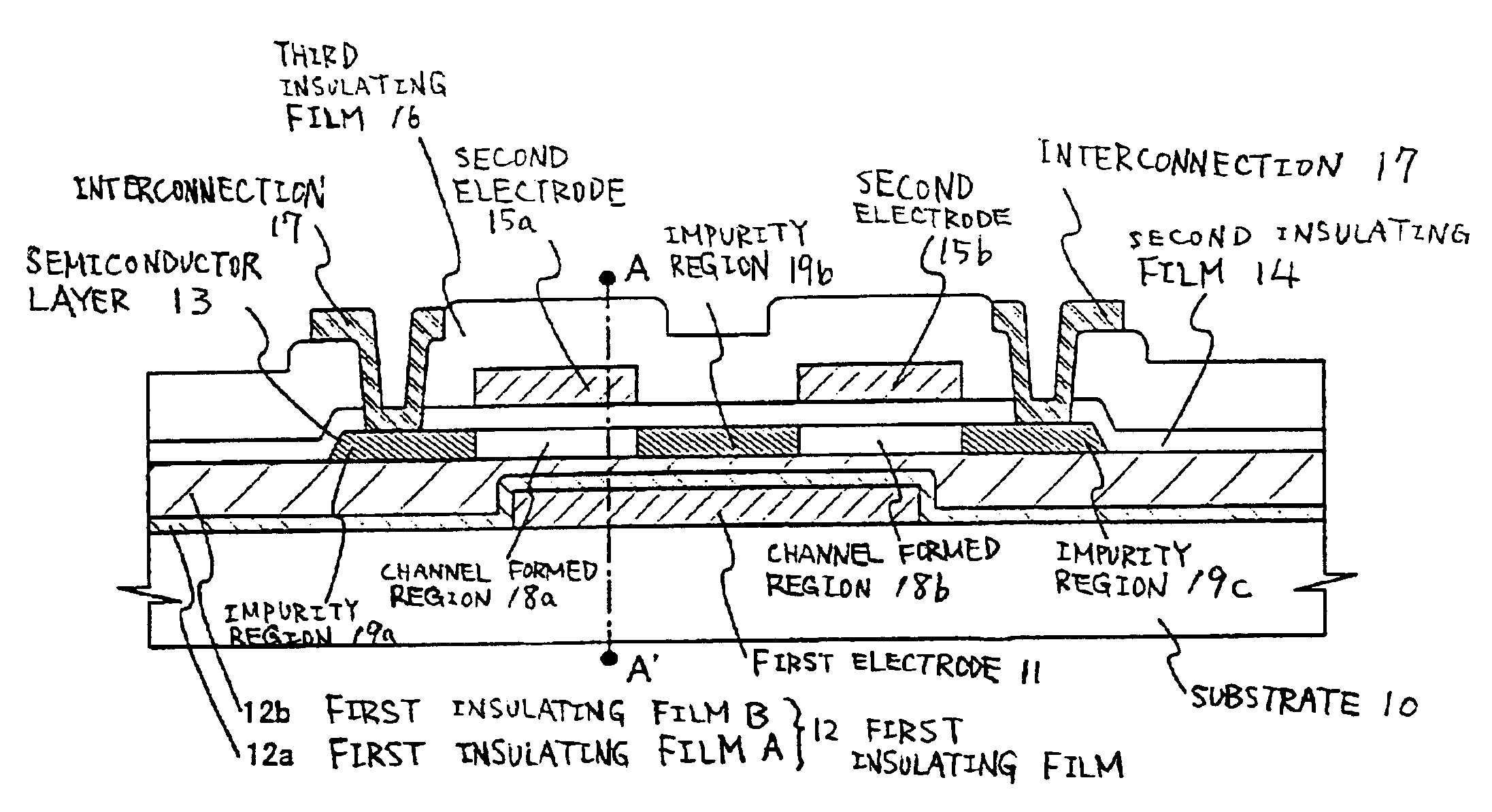
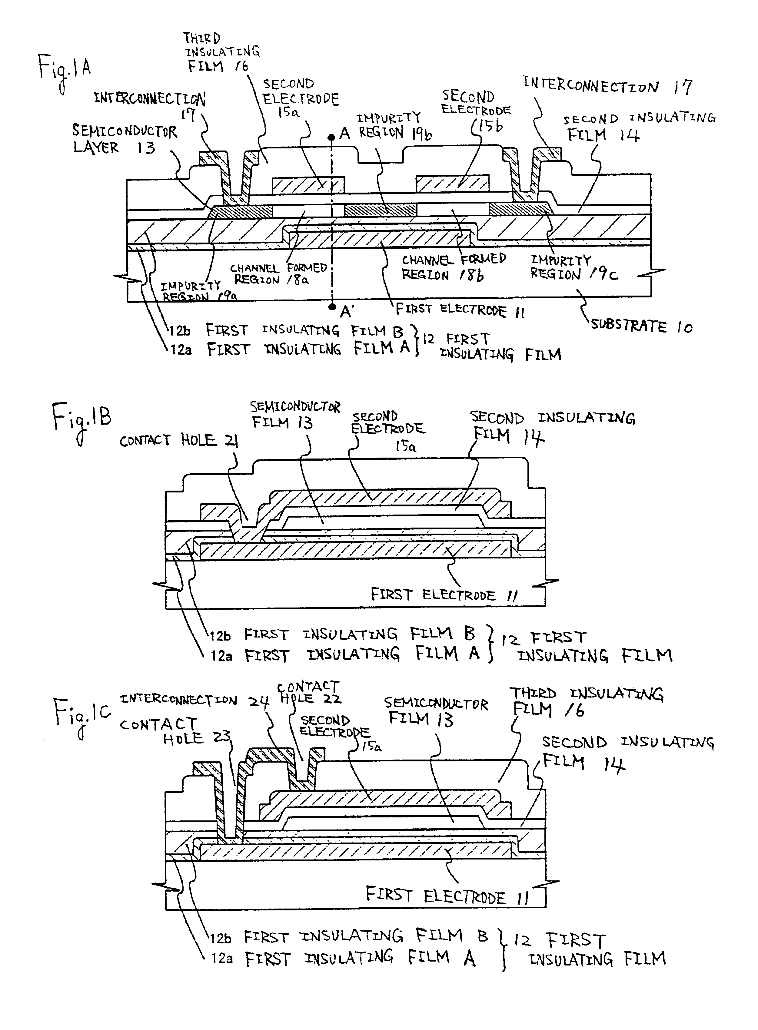
[0109]In this example, an example in which other TFT of the pixel section and TFT formed on a driving circuit have a first electrode and a second electrode, sandwiching a semiconductor layer therebetween, is shown. Only one channel formed region is provided in this example. FIGS. 3A, 3B, 3C to 7A and 7C are cross-sectional views for explaining the semiconductor device manufacturing steps. FIGS. 8A, 8B to FIG. 10 are corresponding top views. For the convenience of explanation, common ...

example 2

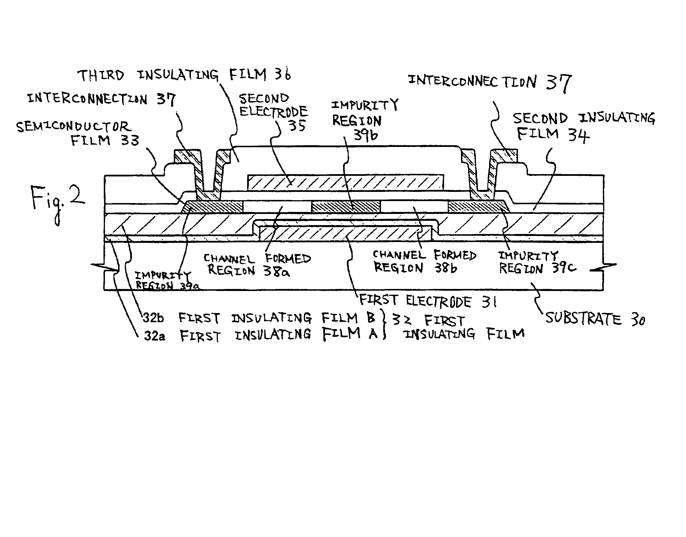
[0150]In this example, the different configuration of the pixels of the light emitting device, which is one example of the semiconductor device according to the present invention from that described in the first example, will be described.

[0151]FIG. 11 is a top view of the pixels of a light emitting device in this example. FIG. 12 is a cross-sectional view taken along line A-A′ of FIG. 11.

[0152]Reference symbol 503 denotes an n-channel type TFT, and 502 denotes a p-channel type TFT. Then-channel type TFT 503 has the first structure of the present invention. The n-channel type TFT 503 includes a semiconductor film 542, a first insulating film 520 (520a and 520b), first electrode 504, a second insulating film 521, and second electrodes 506 and 507. The semiconductor film 542 includes a first concentration, one conductive type impurity regions 508a, 508b, 508c, a second concentration, one conductive type impurity regions 509a, 509b, 509c, 509d and channel formation regions 510 and 511....

example 3

[0159]Another example of the present invention will be described, referring to drawings. One example of the structure of a pixel structure and a driving circuit suitable for a liquid crystal display device will be described. FIGS. 13, 14 and 15, which are referred to in this example, are sectional views for explaining the process of the manufacture thereof. FIGS. 16 and 17 are top views corresponding thereto. In the following description, common reference numbers are used for convenience.

[0160]In FIG. 13A, electrodes 303 to 305 and the first wiring 302 are formed on the substrate 301 in the same way as in Example 1. Then, the first insulating film 307 is formed. In this example, three layers insulating films (the first insulating film A 307a, the first insulating film B 307b and the first insulating film C 307c) are laminated to use as the first insulating film 307. First, a first insulating film A 307a of a silicon oxynitride film is formed to have a thickness of 50 nm. A silicon o...


PUM


Abstract

An object of the present invention is to provide a technique for improving characteristics of a TFT and realizing the structure of the TFT optimal for driving conditions of a pixel section and a driving circuit, using a smaller number of photo masks. A semiconductor device has a semiconductor film, a first electrode, and a first insulating film sandwiched between the semiconductor film and the first electrode, and further has a second electrode, and a second insulating film sandwiched between the semiconductor film and the second electrode. The first electrode and the second electrode overlap with each other across a channel-formed region which the semiconductor film has. A constant voltage is applied to the first electrode at any time.

Description

BACKGROUND OF THE INVENTION[0001]1. Field of the Invention[0002]The present invention relates to a semiconductor device using a thin film transistor (hereinafter referred to as a TFT) wherein a semiconductor film formed on a substrate and having a crystal structure is used; and a process for manufacturing the same. The semiconductor device in the present specification means any device which functions by the use of a semiconductor characteristic, and the category of the semiconductor device manufactured by the present invention includes a display device, a typical example of which is a liquid crystal display device having therein TFTs, and a semiconductor integrated circuit (such as a microprocessor, a signal processing circuit, or a high frequency circuit).[0003]2. Description of Related Art[0004]In various semiconductor devices having therein semiconductor elements, such as a television, a personal computer or a portable telephone, a display for displaying characters or images is a...

Claims


Application Information

Patent Timeline
IPC IPC(8): G02F1/13G02F1/1362H01L21/336H01L29/786H01L21/02H01L21/70H01L29/66H01L21/84H01L27/12H01L21/77
CPCG02F1/136227H01L29/6675H01L29/78621H01L27/1288H01L29/78645H01L29/78648H01L27/124H01L29/78636G02F1/13454
Inventor YAMAZAKI, SHUNPEIOSADA, MAI
Owner SEMICON ENERGY LAB CO LTD
Why Eureka
Try Eureka