Method for forming an electrical interconnection providing improved surface morphology of tungsten

a technology of tungsten and electrical interconnection, which is applied in the direction of semiconductor/solid-state device manufacturing, basic electric elements, electric apparatus, etc., can solve the problems of difficult optimization of process for plug and interconnection stripe application, difficult adjustment of focus, and distortion of the wafer on which the film is deposited, etc., to achieve the effect of easy alignment in the photo process

Inactive Publication Date: 2005-06-21
SAMSUNG ELECTRONICS CO LTD
View PDF8 Cites 51 Cited by
  • Summary
  • Abstract
  • Description
  • Claims
  • Application Information

AI Technical Summary

Benefits of technology

[0010]It is therefore an object of the present invention to provide a method for forming an electrical interconnection that confers the advantageous property of good step coverage in contact holes and low tensile stress in interconnecting stripes, while mitigating, or eliminating, undesirable electrical connection between the interconnecting stripes.
[0015]Because the plug is formed of the lower conductive layer having the property of suitable step coverage, there is substantially no void in the contact hole. Furthermore, since the interconnecting stripe is formed of the upper conductive layer having the attractive property of a smooth surface, there is substantially no residue after the patterning for forming the conductive stripe and therefore accurate alignment in a photo process can be readily obtained.

Problems solved by technology

High tensile stress of a film induces distortion of the wafer on which the film is deposited.
This distortion of the wafer makes an adjustment of focus extremely difficult during a photo process to be performed after the deposition of the film.
Because of the different requirements for tungsten film characteristics and the dependence on process parameters as described above, the optimization of process for both plug and interconnecting stripe application was very difficult.
However, according to the prior art, the anisotropic etching procedure is unable to entirely remove the combination of the two tungsten layers, leaving residue on the dielectric layer.

Method used


Image

  • Method for forming an electrical interconnection providing improved surface morphology of tungsten
  • Method for forming an electrical interconnection providing improved surface morphology of tungsten
  • Method for forming an electrical interconnection providing improved surface morphology of tungsten

Examples


first embodiment

[0027]FIGS. 4 to 9 are cross sectional schematic views illustrating a process for forming an electrical interconnection according to the present invention and FIG. 10 is a cross sectional schematic view illustrating a modified embodiment thereof.

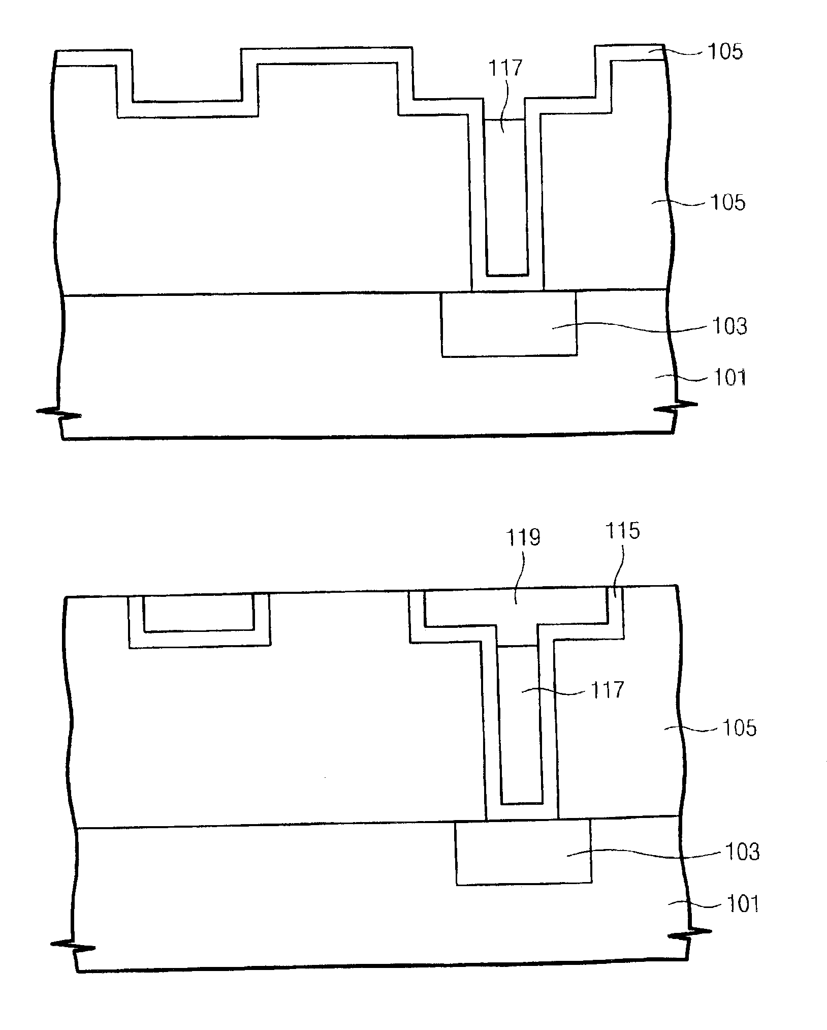
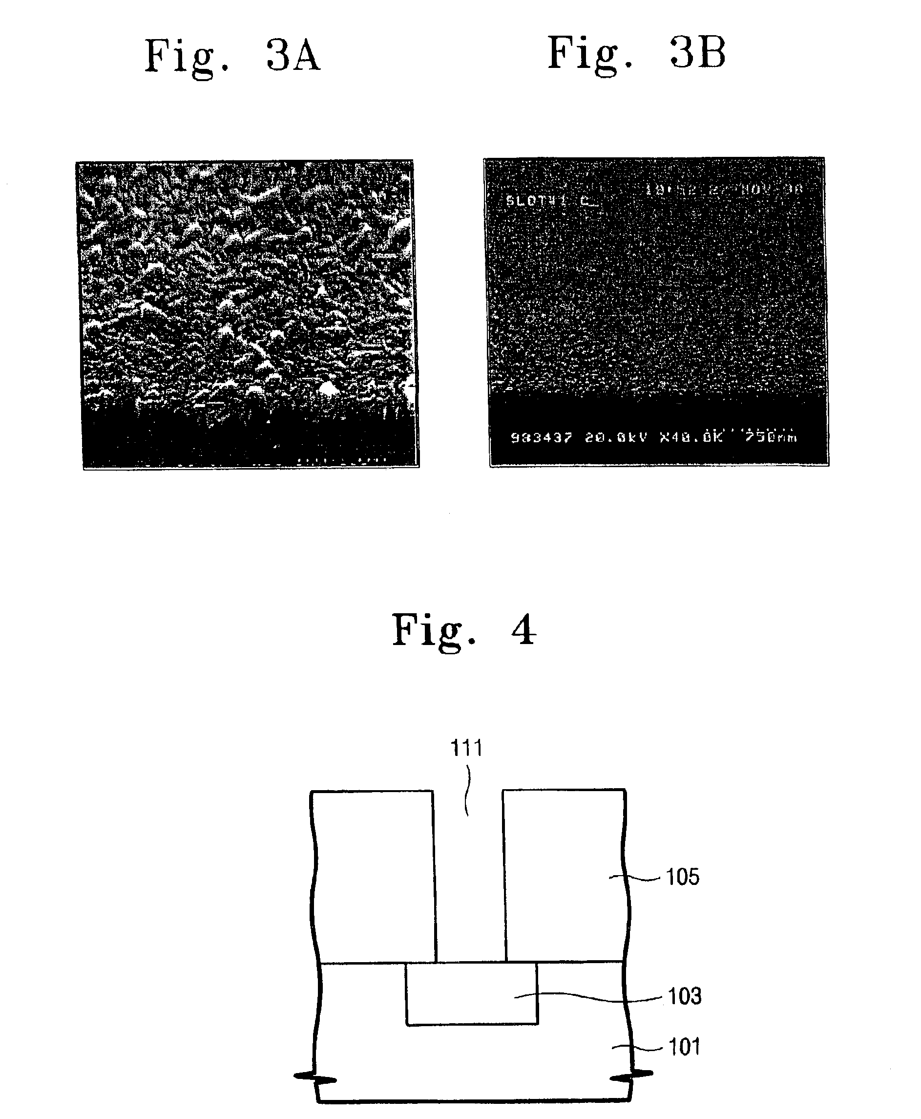
[0028]Referring to FIG. 4, there is shown a substrate 101, preferably composed of monocrystalline silicon. The substrate 101 has a conductive area 103 formed therein. The conductive area 103 is a impurity active region formed by ion implantation into the substrate 101. Other structures such as a polycrystalline silicon pattern, an aluminum wiring pattern, a metal plug or the like, though not shown, may be formed in and on the substrate 101.

[0029]A dielectric layer 105, composed of insulating material such as borophosphosilicate glass (BPSG), spin-on-glass (SOG) or the like, is deposited over the substrate 101 to a thickness of between about 2,000 to 15,000 Angstroms. A contact hole 111 is formed through the dielectric layer 105 to the substr...

second embodiment

[0044]FIGS. 11 and 12 are cross sectional schematic views illustrating a process for forming an electrical interconnection according to the present invention.

[0045]Referring to FIG. 11, a substrate 301, a conductive area 303, a dielectric layer 305, a contact hole 311, a barrier layer 315 and a lower conductive layer 317 are provided using same-method as that of the first embodiment.

[0046]The lower conductive layer 317 and the barrier layer 315 are polished using CMP (chemical mechanical polishing) to expose a surface of the dielectric layer 305 and leave a tungsten plug filling the contact hole.

[0047]Referring to FIG. 12, a second barrier layer 318 is deposited over the dielectric layer 305 and the tungsten plug. The second barrier layer 318 preferably is formed of one selected from the group consisting of titanium, titanium nitride, tungsten silicide and combinations thereof. In this embodiment, the second barrier layer 318 is formed of titanium nitride. This second barrier layer ...


PUM

PropertyMeasurementUnit
thicknessaaaaaaaaaa
pressureaaaaaaaaaa
thicknessaaaaaaaaaa

Abstract

In a fabrication method for forming an electrical interconnection of CVD tungsten film, a contact hole is formed in a dielectric layer. A lower conductive layer is formed in the contact hole and over the dielectric layer. A portion of the lower conductive layer is removed. As a result, the dielectric layer is exposed. An upper conductive layer is formed over the lower conductive layer and over the dielectric layer. The lower conductive layer has a rough surface and the upper conductive layer has a smooth surface. In this manner, following patterning of conductive stripes over the conductive layer, residue is mitigated, and thus, inadvertent interconnection of neighboring stripes is eliminated.

Description

RELATED APPLICATIONS[0001]This application is a continuation-in-part application of U.S. Ser. No. 09 / 859,823, filed May 17, 2001 ABN, which relies for priority upon Korean Patent Application No. 2000-78998, filed on Dec. 20, 2000, the contents of each being herein incorporated by reference in its entirety.FIELD OF THE INVENTION[0002]The invention relates to methods for the fabrication of semiconductor-devices and more particularly to methods for forming an electrical interconnection of CVD tungsten film.BACKGROUND OF THE INVENTION[0003]Fabrication of semiconductor devices generally involves a procedure of forming thin films and layers of various materials on wafers of base semiconductor materials, and removing selected areas of such films to provide structures and circuitry. Tungsten is one of the materials commonly deposited on wafers during fabrication. Tungsten provides many advantageous features that render it especially amenable for forming electrical interconnections including...

Claims


Application Information

Patent Timeline
Patent Type & Authority Patents(United States)
IPC IPC(8): H01L21/285H01L21/02H01L21/3205
CPCH01L21/32051H01L21/28556
Inventor KOO, KYUNG-BUM
Owner SAMSUNG ELECTRONICS CO LTD
Why Eureka
Try Eureka