Method for imprint lithography using an electric field

a technology of imprint lithography and electric field, applied in the field of methods and systems for imprint lithography, can solve the problems the resolution of methods reaching its limit, and the difficulty of obtaining a light source with sufficient output intensity at these wavelengths, so as to improve the aspect ratio of the structure

Inactive Publication Date: 2005-06-21
CANON KK
View PDF161 Cites 204 Cited by
  • Summary
  • Abstract
  • Description
  • Claims
  • Application Information

AI Technical Summary

Benefits of technology

[0010]The curable liquid is cured by the application of activating light. After the curable liquid is cured, the structures may be further defined by etching the cured liquid. Etching may improve the aspect ration of the structures. Any of the commonly used etching techniques may be used, including reactive ion etching.

Problems solved by technology

However, it is believed that these methods are reaching their limits in resolution.
At these short wavelengths, many common materials are not optically transparent and therefore imaging systems typically have to be constructed using complicated reflective optics.
Furthermore, obtaining a light source that has sufficient output intensity at these wavelengths is difficult.
Such systems lead to extremely complicated equipment and processes that may be prohibitively expensive.
It is also believed that high-resolution e-beam lithography techniques, though very precise, are too slow for high-volume commercial applications.
Hot embossing techniques face several challenges: i) pressure greater than 10 MPa are typically required to imprint relief structures, ii) temperatures must be greater than the Tg of the polymer film, iii) patterns (in the substrate film) have been limited to isolation trenches or dense features similar to repeated lines and spaces.
Hot embossing is unsuited for printing isolated raised structures such as lines and dots.
This is because the highly viscous liquids resulting from increasing the temperature of the substrate films require extremely high pressures and long time durations to move the large volume of liquids needed to create isolated structures.
This pattern dependency makes hot embossing unattractive.
Also, high pressures and temperatures, thermal expansion, and material deformation generate severe technical challenges in the development of layer-to-layer alignment at the accuracies needed for device fabrication.
Such pattern placement distortions lead to problems in applications such as patterned magnetic media for storage applications.
The addressing of the patterned medium bit by the read-write head becomes very challenging unless the pattern placement distortions can be kept to a minimum.

Method used


Image

  • Method for imprint lithography using an electric field
  • Method for imprint lithography using an electric field
  • Method for imprint lithography using an electric field

Examples


Embodiment Construction

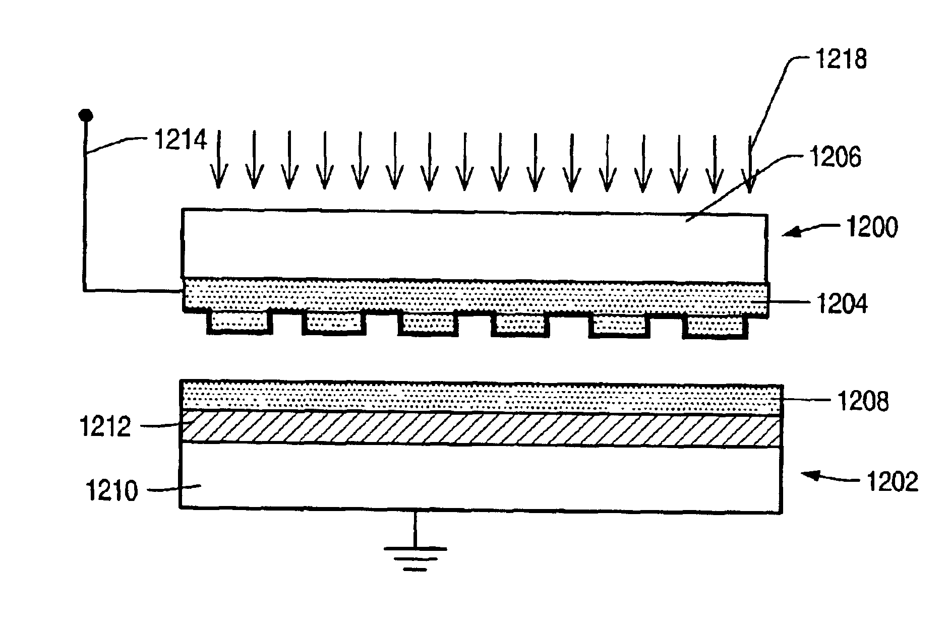
[0053]Embodiments presented herein generally relate to systems, devices, and related processes of manufacturing small devices. More specifically, embodiments presented herein relate to systems, devices, and related processes of imprint lithography. For example, these embodiments may be used for imprinting sub 100 nm features on a substrate, such as a semiconductor wafer. It should be understood that these embodiments may also be used to manufacture other kinds of devices including, but not limited to: patterned magnetic media for data storage, micro-optical devices, micro-electro-mechanical system, biological testing devices, chemical testing and reaction devices, and X-ray optical devices.

[0054]Imprint lithography processes have demonstrated the ability to replicate high-resolution (sub-50 nm) images on substrates using templates that contain images as topography on their surfaces. Imprint lithography may be used in patterning substrates in the manufacture of microelectronic device...


PUM

PropertyMeasurementUnit
viscosityaaaaaaaaaa
surface energyaaaaaaaaaa
wavelengthsaaaaaaaaaa

Abstract

A lithography process for creating patterns in an activating light curable liquid using electric fields followed by curing of the activating light curable liquid is described. The process involves the use of a template that is formed of non-conductive and electrically conductive portions. The template is brought into close proximity to the activating light curable liquid on the substrate. An external electric field is applied to the template-substrate interface while maintaining a uniform, carefully controlled gap between the template and substrate. This causes the activating light curable liquid to be attracted to the raised portions of the template. Activating light is applied to the curable liquid while an electric field is applied to the template to create a patterned layer on the substrate.

Description

BACKGROUND OF THE INVENTION[0001]1. Field of the Invention[0002]Embodiments presented herein relate to methods and systems for imprint lithography. More particularly, embodiments relate to methods and systems for micro- and nano-imprint lithography processes.[0003]2. Description of the Relevant Art[0004]Optical lithography techniques are currently used to make most microelectronic devices. However, it is believed that these methods are reaching their limits in resolution. Sub-micron scale lithography has been a critical process in the microelectronics industry. The use of sub-micron scale lithography allows manufacturers to meet the increased demand for smaller and more densely packed electronic circuits on chips. It is expected that the microelectronics industry will pursue structures that are as small or smaller than about 50 nm. Further, there are emerging applications of nanometer scale lithography in the areas of opto-electronics and magnetic storage. For example, photonic crys...

Claims


Application Information

Patent Timeline
Patent Type & Authority Patents(United States)
IPC IPC(8): B81C1/00G03F7/00H01L21/027H01L21/02
CPCB81C1/0046B82Y10/00H01L21/0271G03F7/0002B82Y40/00
Inventor SREENIVASAN, SIDLGATA V.BONNECAZE, ROGER T.WILLSON, CARLTON GRANT
Owner CANON KK
Why Eureka
Try Eureka