Low jitter clock for a physical media access sublayer on a field programmable gate array

a sublayer and physical media access technology, applied in the field of multi-gigabit transceivers, can solve the problems of adding an unacceptable amount of jitter to the clock signal, and the routing system used by plds does not typically provide clock signals, so as to achieve the effect of increasing the flexibility of the mgt, reducing jitter, and reducing delay

Inactive Publication Date: 2005-06-28
XILINX INC
View PDF5 Cites 24 Cited by
  • Summary
  • Abstract
  • Description
  • Claims
  • Application Information

AI Technical Summary

Benefits of technology

[0011]The PLD also includes general-purpose clock pads for receiving one or more general-purpose clock signals. These general-purpose clock signals are stepped down from the I / O supply voltage level to the core logic supply voltage level, and routed to the clock multiplexer circuits of the MGTs on the standard global clock routing circuitry of the PLD. The clock multiplexer circuits also allow the general-purpose clock signals to be routed as reference clock signals for the MGTs. The clock multiplexer circuits include up-level shifters for stepping up the general-purpose clock signals from the core logic supply voltage level to the I / O supply voltage level. While the general-purpose clock signals provide reference clock signals having higher jitter than the high-quality differential clock signals, allowing for the use of the general-purpose clock signals advantageously increases the flexibility of the MGT. That is, a designer can choose to use a less expensive clock source, or may choose to use either single-ended or differential clock signals when using the general-purpose clock pads.
[0012]In addition to the clock multiplexer circuitry, each MGT includes a physical media access (PMA) sublayer and a physical coding sublayer (PCS). As described above, the clock multiplexer circuitry routes one of the high-quality differential clock signals or general-purpose clock signals as a reference clock signal. This reference clock signal is used to control the serializing and deserializing of data within the PMA. This reference clock signal is also stepped down to the core logic supply voltage level by a down-level shifter to provide a PCS reference clock signal that controls the PCS. The down-level shifter advantageously adds a slight delay to the reference clock signal, such that the PCS reference clock signal is able to eliminate hold time issues on the data flowing from the PCS to the PMA.

Problems solved by technology

One reason for this is that the clock routing systems used by PLDs do not typically provide clock signals having jitter low enough to support multi-gigabit operation.
These stepping down and stepping up processes add an unacceptable amount of jitter to the clock signals.

Method used


Image

  • Low jitter clock for a physical media access sublayer on a field programmable gate array
  • Low jitter clock for a physical media access sublayer on a field programmable gate array
  • Low jitter clock for a physical media access sublayer on a field programmable gate array

Examples


Embodiment Construction

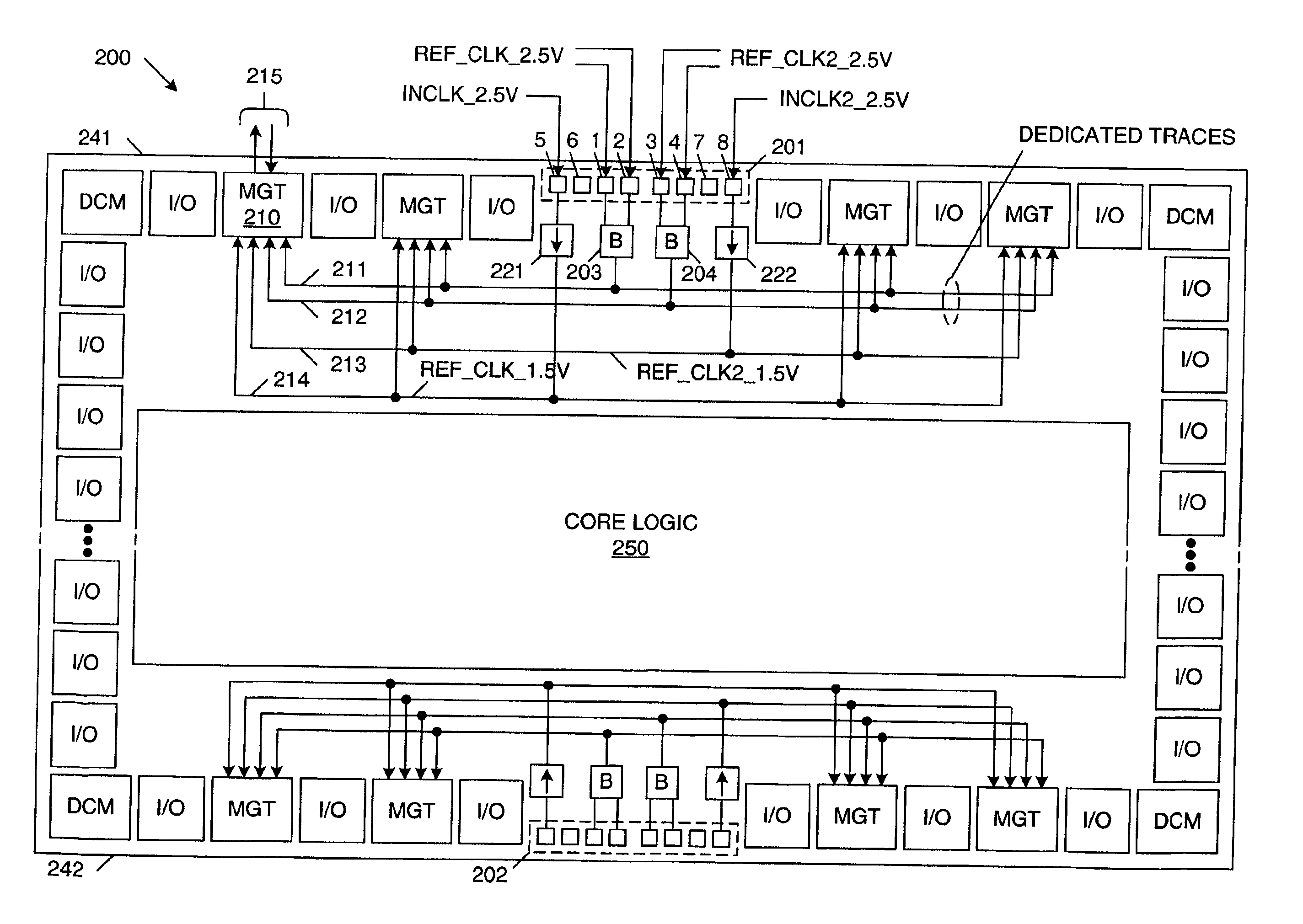
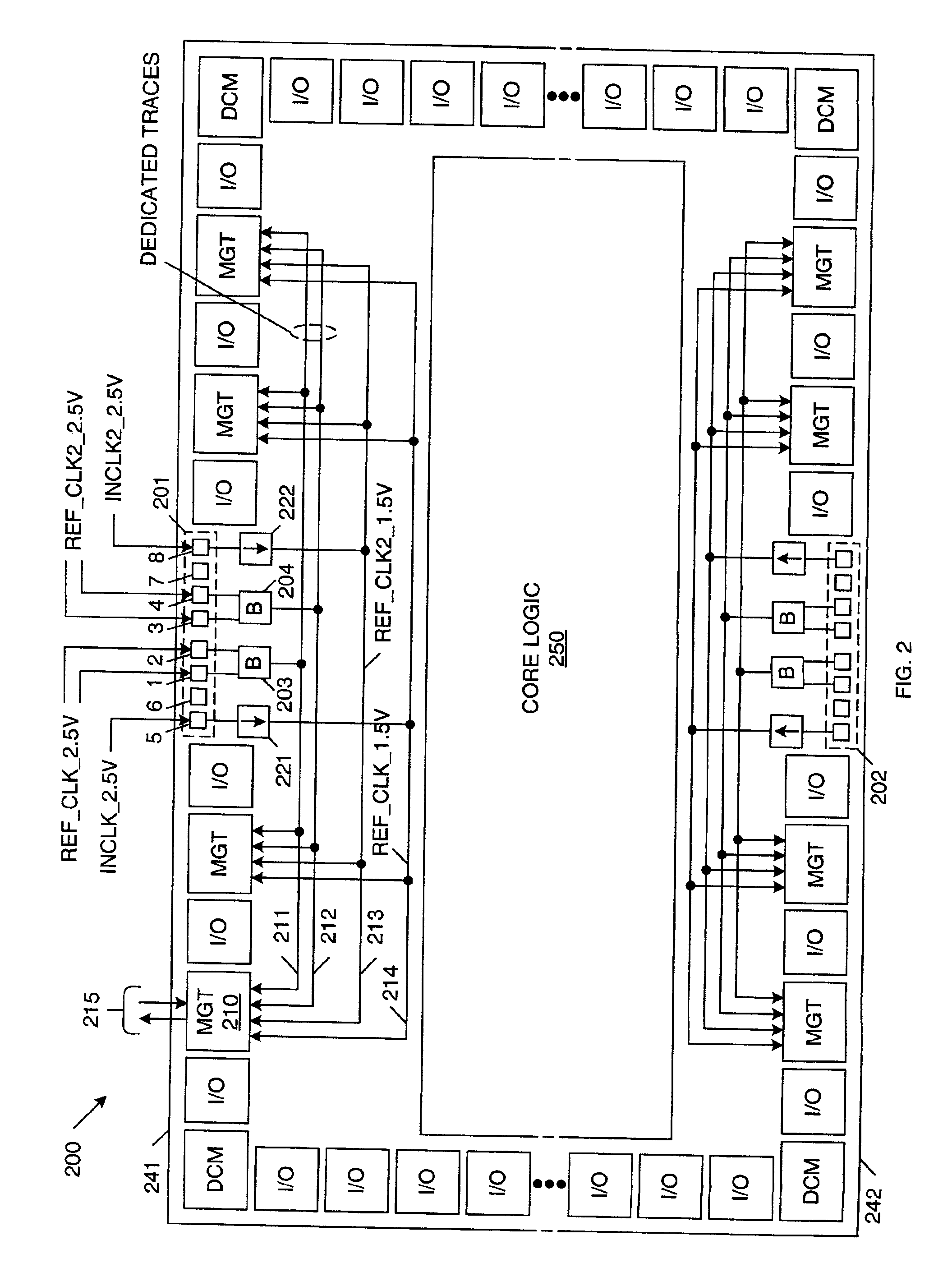
[0018]FIG. 2 is a block diagram of a programmable logic device (PLD) 200 in accordance with one embodiment of the present invention. In the described embodiment, PLD 200 is a field programmable gate array (FPGA) that includes select I / O blocks (labeled I / O), digital clock managers (labeled DCM) and multi-gigabit transceivers (labeled MGT) located around the perimeter of the device (i.e., the I / O region). PLD 200 also includes core logic 250 (i.e., the core region), which includes an array of configurable logic blocks (CLBs) and programmable routing circuitry, in the described embodiment. Select I / O blocks, digital clock managers and core logic are well known to those of ordinary skill in the art. These elements of PLD 200 are described in detail in “Virtex™-II Platform FPGA Handbook”, December 2000, pp 33-75, available from Xilinx Inc., 2100 Logic Drive, San Jose, Calif. 95124.

[0019]Elements in the I / O region operate in response to an I / O supply voltage, and elements in the core reg...


PUM


Abstract

A programmable logic device (PLD) is provided that supports multi-gigabit transceivers (MGTs). The PLD includes one or more pairs of shared clock pads for receiving one or more high-quality differential clock signals. Dedicated clock traces couple each pair of shared clock pads to one or more MGTs on the PLD. Each MGT includes a clock multiplexer circuit, which allows one of the high-quality differential clock signals to be routed as a reference clock signal for the MGT. The clock multiplexer circuits are designed such that no significant jitter is added to the high-quality clock signals. The clock multiplexer circuits can also route general-purpose clock signals received by the PLD as lower quality reference clock signals for the MGTs. The reference clock signal routed by the clock multiplexer circuit can be stepped down to provide a reference clock for a physical coding sublayer of the MGT.

Description

BACKGROUND OF THE INVENTION[0001]1. Field of the Invention[0002]The present invention relates to multi-gigabit transceivers (MGTS) located on a programmable logic device (PLD), such as a field programmable gate array (FPGA). More specifically, the present invention relates to a method and apparatus for providing low jitter clock signals for use in the operation of an MGT on a PLD.[0003]2. Related Art[0004]FIG. 1 is a simplified block diagram of a portion of a conventional multi-gigabit transceiver (MGT) 100. The illustrated elements of MGT 100 include serializer 101, deserializer 102 and transmit phase locked loop (PLL) 111. It is understood by those of ordinary skill that conventional MGT 100 includes many other elements in addition to those illustrated in FIG. 1.[0005]In general, MGT 100 operates as an input / output (I / O) interface between serial channel 121 and parallel channel 122. Thus, parallel data (N-bits wide in the described example) is provided to serializer 101 at a first...

Claims


Application Information

Patent Timeline
Patent Type & Authority Patents(United States)
IPC IPC(8): G06F1/10G06F1/04H03K17/693H03K19/173
CPCG06F1/10
Inventor GHIA, ATUL V.VADI, VASISHT M.BEKELE, ADEBABAY M.COSTELLO, PHILIP D.VERMA, HARE K.
Owner XILINX INC
Why Eureka
Try Eureka