Pattern formation method
a pattern and formation method technology, applied in the field of pattern formation methods, can solve the problems of large exposure energy required in any of the conventional methods, insufficient extreme ultraviolet resistance of conventional chemically amplified resist materials, and disadvantageous poor throughput of lithography in the semiconductor fabrication process
- Summary
- Abstract
- Description
- Claims
- Application Information
AI Technical Summary
Benefits of technology
Problems solved by technology
Method used
Image
Examples
embodiment 1
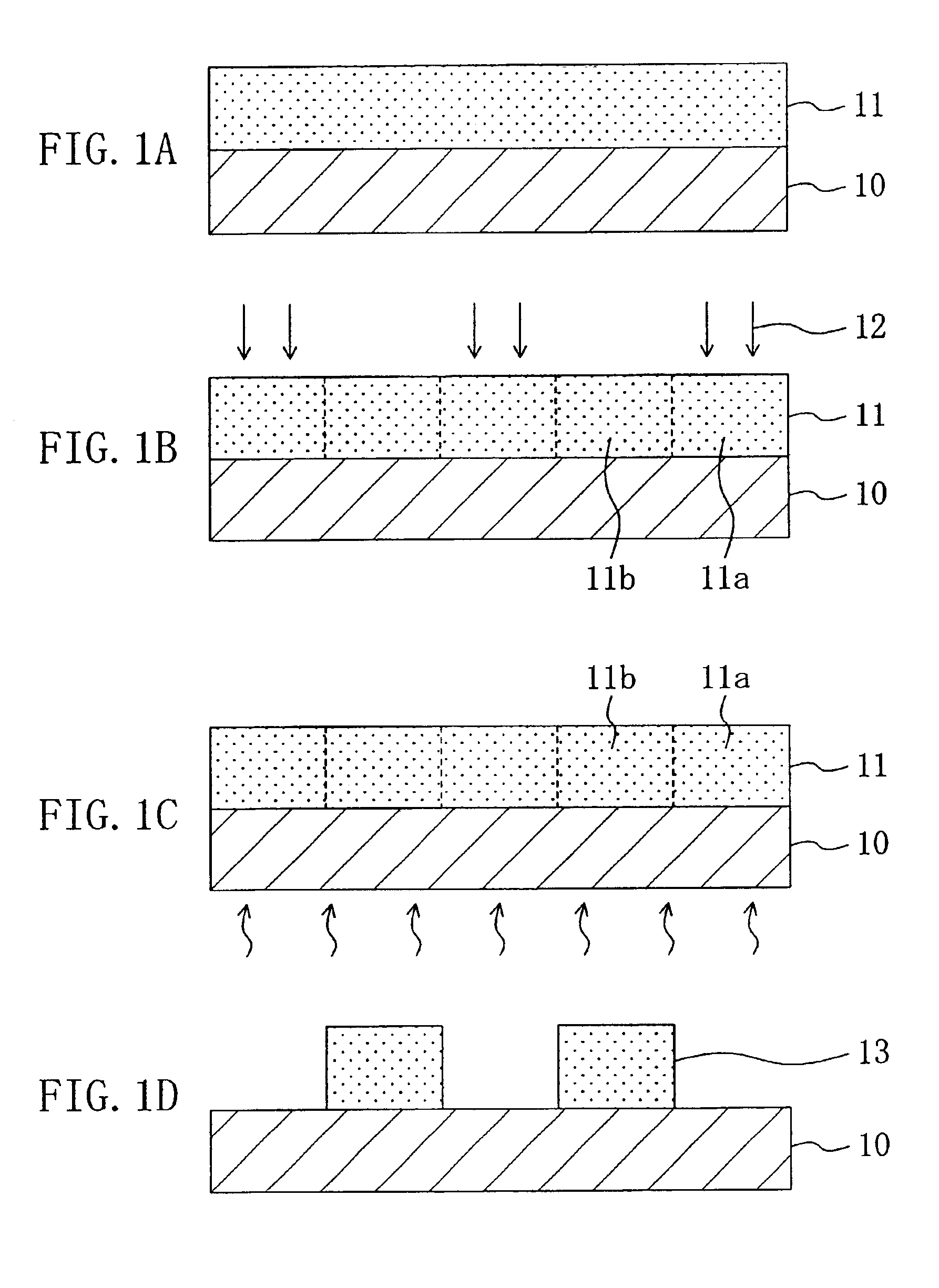
[0038]A pattern formation method according to Embodiment 1 of the invention will now be described with reference to FIGS. 1A through 1D.
[0039]First, a chemically amplified resist material having the following composition is prepared:
[0040]
Phenol polymer: poly((t-butyloxystyrene) − (hydroxystyrene))1.8 g(wherein t-butyloxystyrene:hydroxystyrene = 40 mol %:60 mol %)Acrylic polymer: poly(acrylic acid)0.2 gOnium salt: triphenylsulfonium triflate0.4 gSolvent: propylene glycol monomethyl ether acetate20 g
[0041]Next, as shown in FIG. 1A, the chemically amplified resist material having the aforementioned composition is applied on a semiconductor substrate 10, so as to form a resist film 11. Then, as shown in FIG. 1B, the resist film 11 is selectively irradiated for pattern exposure with extreme UV 12 (of a wavelength of a 13.5 nm band) with exposure energy of 8 mJ / cm2 through a reflection mask (not shown).
[0042]After the pattern exposure, the resist film 11 is subjected to post-exposure bak...
embodiment 2
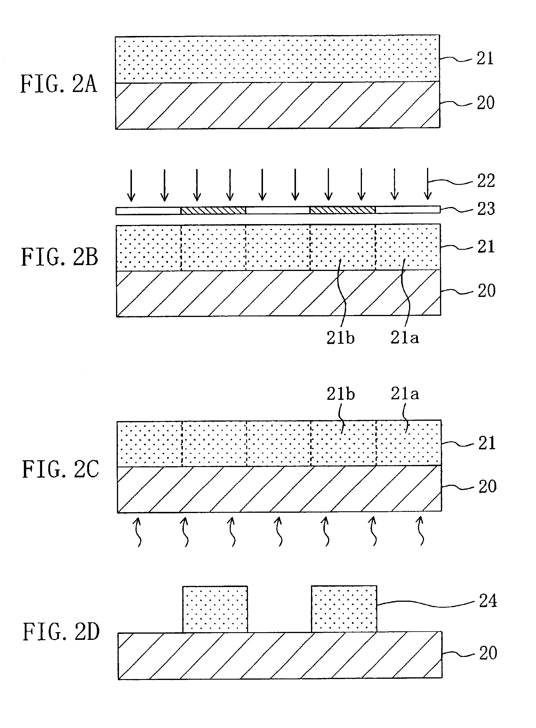
[0045]A pattern formation method according to Embodiment 2 of the invention will now be described with reference to FIGS. 2A through 2D.
[0046]First, a chemically amplified resist material having the following composition is prepared:
[0047]
Phenol polymer: poly((t-butyloxycarbonyloxystyrene) − (hydroxy-1.8 gstyrene)) (wherein t-butyloxycarbonyloxystyrene:hydroxystyrene =35 mol %:65 mol %)Acrylic compound: acrylic acid0.3 gOnium salt: triphenylsulfonium triflate0.8 gSolvent: propylene glycol monomethyl ether acetate20 g
[0048]Next, as shown in FIG. 2A, the chemically amplified resist material having the aforementioned composition is applied on a semiconductor substrate 20, so as to form a resist film 21. Then, the resist film 21 is selectively irradiated for pattern exposure with an electron beam 22 with exposure energy of 5 μC / cm2 through a mask 23.
[0049]After the pattern exposure, the resist film 21 is subjected to post-exposure bake (PEB) by annealing the substrate 20 with a hot plat...
PUM
| Property | Measurement | Unit |
|---|---|---|
| wavelength | aaaaa | aaaaa |
| wavelength | aaaaa | aaaaa |
| wavelength | aaaaa | aaaaa |
Abstract
Description
Claims
Application Information


