

Organic thin-film transistor manufacturing method, organic thin-film transistor, and organic thin-film transistor sheet
a technology of organic thin film transistors and manufacturing methods, applied in the direction of optics, solid-state devices, instruments, etc., can solve the problems of lowering transistor properties, large-sized display panels, and large increase in manufacturing costs or running costs, so as to minimize deterioration, deterioration, and deterioration with time.
- Summary
- Abstract
- Description
- Claims
- Application Information
AI Technical Summary
Benefits of technology
Problems solved by technology
Method used
Image

Examples
example 1
Preparation of Organic Thin-Film Transistor Samples 1 through 9
(1) Preparation of Organic Thin-Film Transistor Sample 1
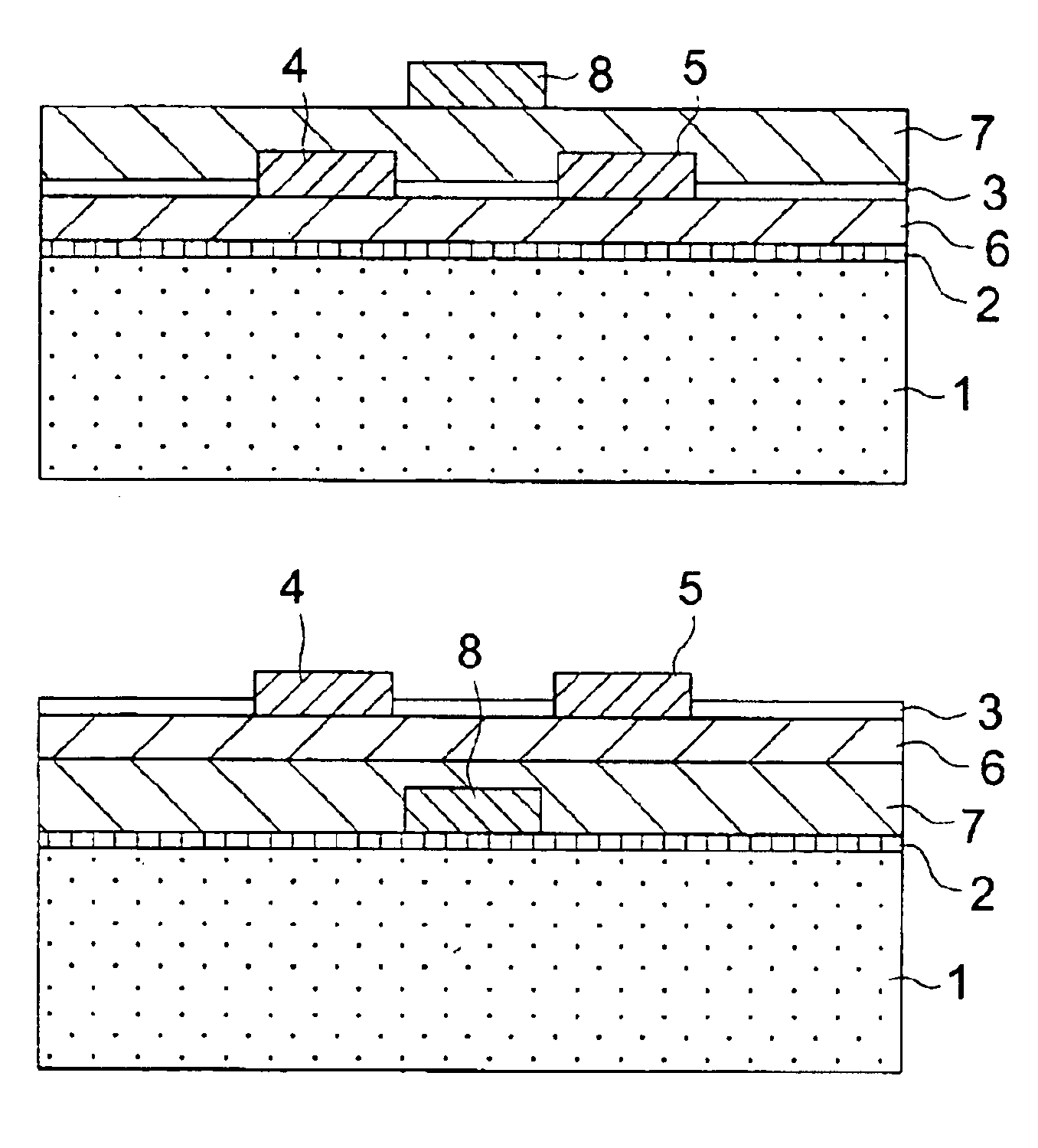
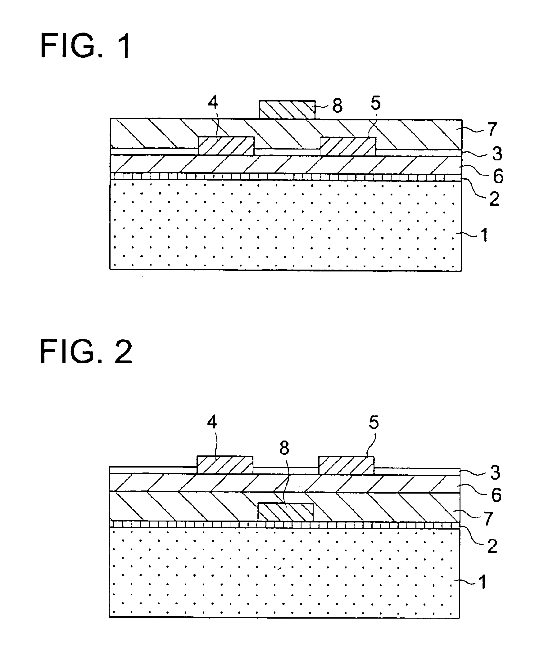
[0177]A mixture of 3.04 g (20 mmol) of tetramethoxysilane, 1.52 g of methylene chloride, and 1.52 g of ethanol was mixed with 0.72 g of an aqueous 0.5% by weight nitric acid solution for hydrolysis, and stirred at room temperature for one hour. A solution in which 1.60 g of diacetylcellulose L50 (produced by Daicel Co., Ltd.) was dissolved in a mixed solvent of 5.3 g of ethanol and 60.9 g of methyl acetate was added to the resulting mixture above, and stirred for one hour to obtain a dope. The resulting dope was cast on a moving gum belt through a doctor blade with a gap width of 800 μm, and dried at 120° C. for 30 minutes to obtain a substrate 1 with a thickness of 200 μm. The substrate 1 had a Tg of 226° C., which was obtained by dynamic viscoelastic measurement.
[0178]The surface of substrate 1 was corona discharged at 50 W / m2 / min and then coated with a coating li...
example 2
Evaluation of Organic Thin-Film Transistor Samples 1 through 10
[0209]The organic thin-film transistor sample 1 and organic thin-film transistor samples 5 through 10 exhibited good working property as a p-channel enhancement type FET. With respect to the organic thin-film transistor samples 1 through 10, carrier mobility (cm2 / V·sec), and an ON / OFF ratio (a drain current ratio when a drain bias was −50 V and a gate bias was −50V and 0 V) were determined from a saturation region of I-V characteristic.
[0210]Further, after the organic thin-film transistor samples 1 through 10 were stored in an atmosphere for one month, the carrier mobility and the ON / OFF ratio thereof were determined.
[0211]Each of the organic thin-film transistor samples 1 through 10 was folded while the substrate side of each sample contacted a stainless steel shaft with an R of 10 mm, and then carrier mobility thereof was determined. The results are shown in Table 1.
[0212]
TABLE 1Immediately afterAfter one monthAfterpre...
example 3
Preparation of Organic Thin-Film Transistor Sample 11 and its Evaluation
[0214]Organic thin-film transistor sample 11 was prepared in the same manner as organic thin-film transistor sample 1, except that a mixture layer of polyvinyl alcohol and carbon black (=8:2 by weight) was used as an organic semiconductor layer protective layer instead of the organic semiconductor layer protective layer of polyvinyl alcohol. The resulting mixture layer of polyvinyl alcohol and carbon black had an average light transmittance at visible wavelength regions of 0.1%.
[0215]The organic thin-film transistor sample 10 provided the same good FET property as the organic thin-film transistor sample 1. When the sample 11 immediately after prepared was exposed to light of 500 cd through a tungsten lamp, properties thereof were not changed.
PUM
| Property | Measurement | Unit |
|---|---|---|
| light transmittance | aaaaa | aaaaa |
| light transmittance | aaaaa | aaaaa |
| wavelength | aaaaa | aaaaa |
Abstract
Description
Claims
Application Information