Power semiconductor device having RESURF layer

a technology of semiconductor devices and resurf layers, which is applied in the direction of semiconductor devices, semiconductor/solid-state device details, electrical equipment, etc., can solve the problems of low breakdown voltage, low breakdown voltage, and low breakdown voltag

Inactive Publication Date: 2005-07-19
AMANO CINCINNATI
View PDF18 Cites 84 Cited by
  • Summary
  • Abstract
  • Description
  • Claims
  • Application Information

AI Technical Summary

Benefits of technology

[0014]In the method (1), in forming the RESURF layers 180, crystal growth progresses at the corner portions of a trench bottom portion from both the bottom portion and the side surfaces. For this reason, the crystallinity of the RESURF layer 180 deteriorates at the corner portions of the trench bottom portion. This may make the breakdown voltage low. In addition, since the crystal growth rate in the upper portion differs from that in the lower portion of a trench, a cavity may be generated in the trench. In this case, the thickness of the RESURF layer 180 with a cavity may be different from that of the RESURF layer 180 without any cavity. This may lower the breakdown voltage.

Problems solved by technology

This may result in noise.
This may make the breakdown voltage low.
This may lower the breakdown voltage.
Due to disorder in crystallinity or mixing of an unexpected impurity, the breakdown voltage may become low, or the electrical characteristic may degrade.
That is, to form a thin and deep RESURF layer 180 to reduce the cell width, the crystal growth process and ion implantation process must be repeated many times. This makes the process very complex and also increases the number of growth interfaces.

Method used


Image

  • Power semiconductor device having RESURF layer
  • Power semiconductor device having RESURF layer
  • Power semiconductor device having RESURF layer

Examples


16th embodiment

[0240]A method of manufacturing a semiconductor device according to the 16th embodiment of the present invention will be described next with reference to FIGS. 23A and 23B. FIGS. 23A and 23B are sectional views sequentially showing steps in manufacturing a power MOS transistor according to this embodiment.

[0241]First, the structure shown in FIG. 22A is obtained by the process described in the 15th embodiment. That is, before a trench TG is completely filled with a second drift layer 33, crystal growth of the second drift layer 33 is stopped.

[0242]Next, high-temperature annealing in a hydrogen atmosphere is executed. As a result, silicon atoms near the surface of the second drift layer 33 are diffused to fill and planarized the unfilled portion of the trench TG. Thus, the number of crystal defects at the interface in the second drift layer 33 is decreased. When the trench TG is filled using high-temperature annealing in a hydrogen atmosphere, cavities 35 may be formed, as shown in FI...

18th embodiment

[0252]A method of manufacturing a semiconductor device according to the 18th embodiment of the present invention will be described next with reference to FIGS. 25A to 25D. FIGS. 25A to 25D are sectional views sequentially showing steps in manufacturing a vertical power MOS transistor according to this embodiment.

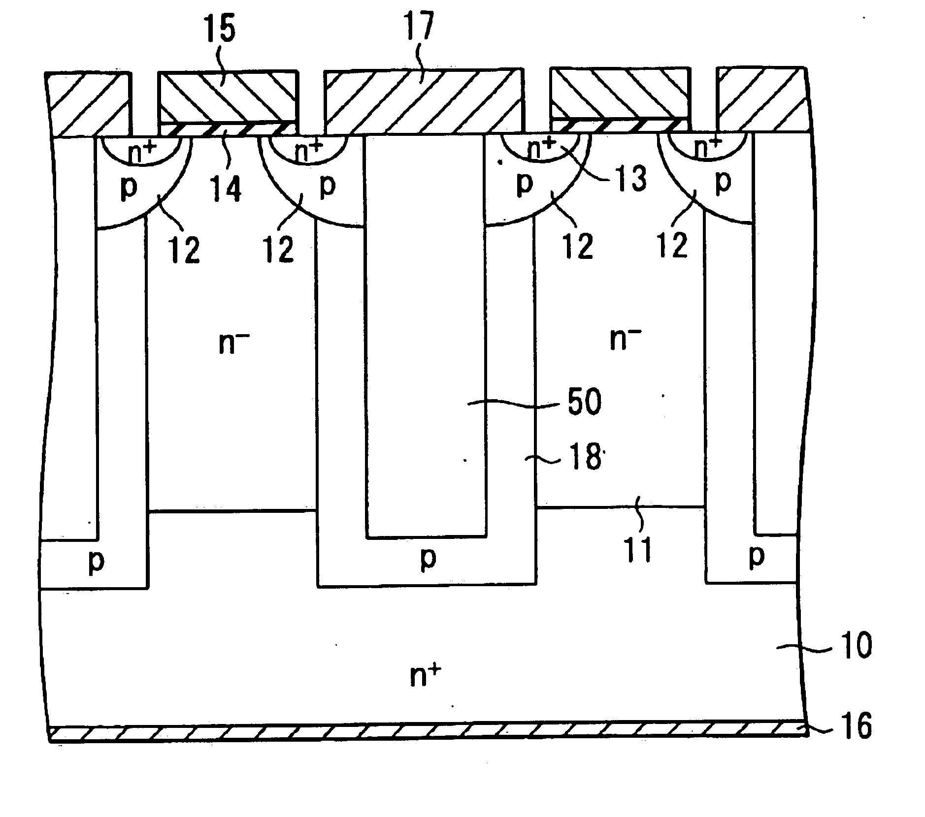
[0253]First, the structure shown in FIG. 20C is obtained by the process described in the 14th embodiment. An n-type impurity such as phosphorus or arsenic is implanted into the side walls of RESURF layers 18. To implant the impurity, ion implantation from oblique directions with respect to the side walls of the trench or a method such as vapor phase diffusion or solid phase diffusion can be used.

[0254]As shown in FIG. 25B, the n-type impurity is activated by activation annealing to form second drift layers 33.

[0255]When high-temperature annealing is performed in a hydrogen atmosphere, atoms in the inner walls of a trench TG move. The atoms that form the RESURF layers 18 and ...

23rd embodiment

[0282]A semiconductor device according to the 23rd embodiment of the present invention will be described next with reference to FIG. 30. FIG. 30 is a sectional view of a vertical power MOS transistor according to this embodiment. This embodiment is related to the structure of an element terminating portion of a vertical power MOS transistor.

[0283]As shown in FIG. 30, in the structure according to this embodiment, guard rings 41 in the structure shown in FIG. 27B described in the 20th embodiment are omitted. Instead, a p-type RESURF layer 46 is formed in the surface regions of a first drift layer 11, guard rings 39, and n−-type semiconductor layers 40. The RESURF layer 46 commonly connects the pairs of guard rings 39 and is connected to a base layer 12.

[0284]According to the above arrangement, when the width of the RESURF layer 46 is set to 100 μm, and the impurity dose is set to 8×1011 cm−2, a MOS transistor having a breakdown voltage of 600V can be implemented. The planar pattern o...


PUM


Abstract

A semiconductor device including a drain layer having a first conductivity type, a drift layer having the first conductivity type, which is formed on the drain layer and has an impurity concentration lower than that in the drain layer, and a RESURF layer having a second conductivity type and formed to extend from a surface of the drift layer into the drain layer, the RESURF layer forming a superjunction structure together with the drift layer and forming a depletion layer in the drift layer.

Description

CROSS-REFERENCE TO RELATED APPLICATIONS[0001]This application is based upon and claims the benefit of priority under 35 USC §119 from the prior Japanese Patent Applications No. 2001-175041, filed Jun. 11, 2001; No. 2001-276801, filed Sep. 12, 2001; No. 2001-298311, filed Sep. 27, 2001, and under 35 USC §120 from U.S. Ser. No. Div. 10 / 163,651, filed Jun. 7, 2002 U.S. Pat. No. 6,693,338 the entire contents of all of which are incorporated herein by reference.BACKGROUND OF THE INVENTION[0002]1. Field of the Invention[0003]The present invention relates to a semiconductor device having a RESURF (REduced SURface Field) layer and, more particularly, to a technology applied to a high-power semiconductor device.[0004]2. Description of the Related Art[0005]Conventionally, vertical power MOS-transistors are widely known. The ON resistance of a vertical power MOS transistor greatly depends on the electrical resistance of a conducting layer (drift layer) portion. The electrical resistance of a d...

Claims


Application Information

Patent Timeline
Patent Type & Authority Patents(United States)
IPC IPC(8): H01L21/336H01L29/78H01L21/02H01L29/66H01L21/265H01L29/06H01L29/08H01L29/02
CPCH01L21/3247H01L29/0634H01L29/0878H01L29/66712H01L29/7802H01L29/7811H01L29/7816H01L21/26586H01L29/0615H01L29/0619H01L29/0653H01L29/0696H01L29/1095H01L29/402H01L29/41741H01L29/7824H01L2924/0002H01L2924/00H01L29/78
Inventor SAITOH, WATARUOMURA, ICHIRO
Owner AMANO CINCINNATI
Why Eureka
Try Eureka