Display device and method of manufacturing the same

a technology of display panel and manufacturing method, which is applied in the field of display panel, can solve the problems of not meeting the need for the above-mentioned technical trend, difficult to form ultra-high-definition display panel, and difficult to build peripheral circuit in the frame region, so as to reduce the occupied area of semiconductor circuit made of tfts, reduce the alignment margin, and eliminate the margin required to add impurities.

Inactive Publication Date: 2005-07-19
SHARP KK
View PDF11 Cites 94 Cited by
  • Summary
  • Abstract
  • Description
  • Claims
  • Application Information

AI Technical Summary

Benefits of technology

[0036]According to the present invention, the n-type MOS transistor and the p-type MOS transistor employed in the CMOS circuit are formed in the same island-like semiconductor layer. Therefore, the margin region required to add the impurity can be eliminated, and also the occupied area of the semiconductor circuit made of TFTs can be reduced.
[0037]In addition, since the boundary between the mutually contact impurity introduced regions of the n-type TFT and the p-type TFT is formed zigzag, the holes formed on the boundary between these impurity introduced regions are hard to deviate to one side. Therefore, the alignment margin can be reduced and thus the occupied area of the CMOS circuit can be further reduced.
[0038]Also, according to the present invention, since at least ones of the mutually adjacent impurity introducing regions of the n-type TFT and the p-type TFT formed in the same pattern region are shared to contact, the design area of the CMOS circuit can be much more reduced.
[0039]Accordingly, since the high performance / multiple function large-scale semiconductor integrated circuits such as the digital driver, DAC, the memory, the I / O circuit, the data processing circuit, CPU, etc. can be built in the ultra high-definition display device, the high performance display device can be manufactured. Also, since the semiconductor integrated circuit can be housed in the narrow peripheral frame region of the display device, the narrower frame, the lighter weight and the compactness of the display device in which the peripheral circuit is integrally formed can be achieved. In addition, even if the manufacturing equipment with the relatively low processing precision is employed, the relatively high integration density can be obtained and therefore the significant reduction in the production cost of the display device in which the peripheral circuit is integrally formed can be achieved.

Problems solved by technology

By the way, the liquid crystal display panel, in which the peripheral circuit employing the low-temperature polysilicon in the prior art is built, cannot answer the need for the above technical trend because of following subjects.
It is difficult to form the ultra high-definition display panel, in which the digital driver is built and which has 200 dpi or more, by the manufacturing method in the prior art.
Therefore, in the case of the ultra high-definition panel having the narrow frame, it becomes difficult to built the peripheral circuit in the frame region.
Also, it is difficult for the existing large-size pattern forming system (the etching equipment, etc.) to form respective metal layer patterns with the working precision of less than 2 μm.

Method used


Image

  • Display device and method of manufacturing the same
  • Display device and method of manufacturing the same
  • Display device and method of manufacturing the same

Examples


first embodiment

[0057](First Embodiment)

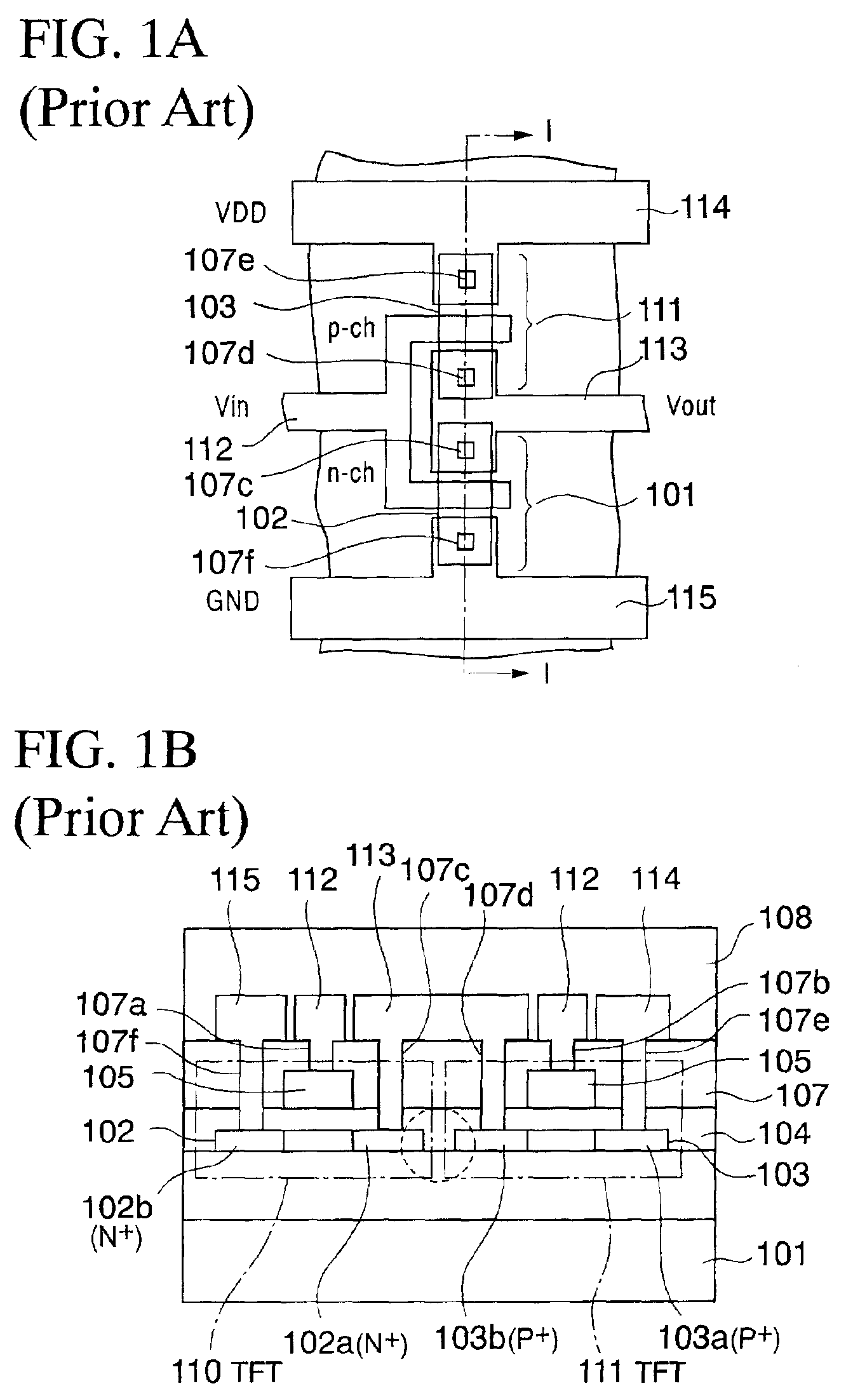
[0058]In the first embodiment, a CMOS inverter and a CMOS analog switch both having a configuration, in which one n-type impurity diffusion region constituting an n-channel TFT and one p-type impurity diffusion region constituting a p-channel TFT are not separated but formed continuously and adjacently on one silicon island, will be explained hereunder.

[0059](i) CMOS Inverter

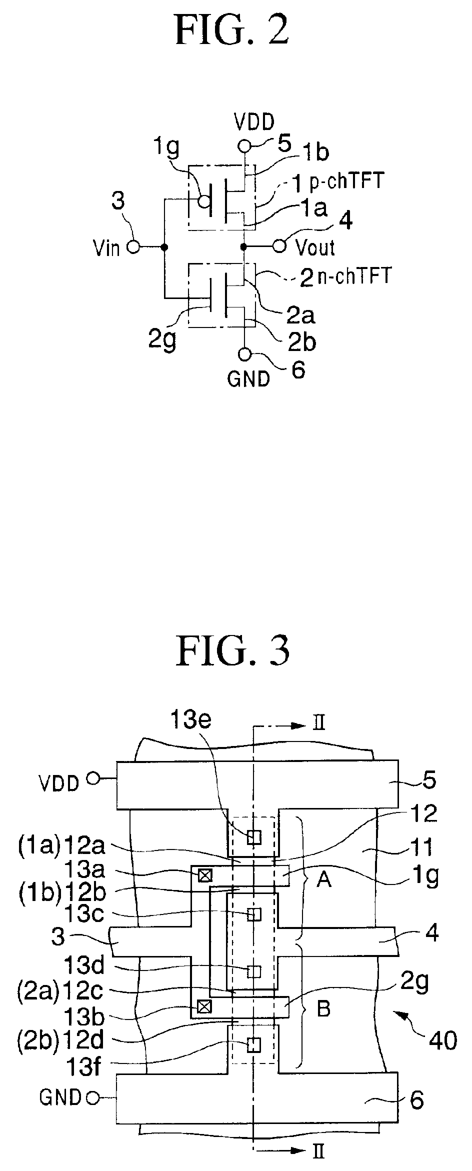
[0060]FIG. 2 is an equivalent circuit diagram showing a CMOS inverter. In FIG. 2, gate electrodes 1g, 2g of a p-channel thin film transistor (p-ch TFT) 1 and an n-channel thin film transistor (n-ch TFT) 2 are connected to the same input wiring 3 respectively. Also, a second source / drain 1a of the p-ch TFT 1 and a first source / drain 2a of the n-ch TFT 2 are connected to the same output wiring 4. In addition, a first source / drain 1b of the p-ch TFT 1 is connected to a power supply wiring 5, and a second source / drain 2b of the n-ch TFT 2 is connected to a ground wiring 6.

[0061]FIG. 3 is a pl...

second embodiment

[0104](Second Embodiment)

[0105]In a second embodiment, a CMOS TFT having such a configuration that mutually neighboring source / drain regions of the p-channel thin film transistor and the n-channel thin film transistor are formed continuously not to leave a space between them and neighboring n-type source / drain and p-type source / drain are connected to the same wiring via one contact hole will be explained hereunder.

[0106]FIG. 7 is a plan view showing a layout of a CMOS inverter according to a second embodiment of the present invention, and FIG. 8 is a sectional view taken along a IV—IV line in FIG. 7. In FIG. 7 and FIG. 8, the same references as those in FIG. 3 and FIG. 6J denote the same elements.

[0107]A CMOS inverter 41 in FIG. 7 employs the p-ch TFT 1 and the n-ch TFT 2 disclosed in the first embodiment, and has such a configuration that a contact hole 13h is formed at the boundary portion between a second p+-type impurity region 12b serving as one source / drain of the p-ch TFT 1 a...

third embodiment

[0114](Third Embodiment)

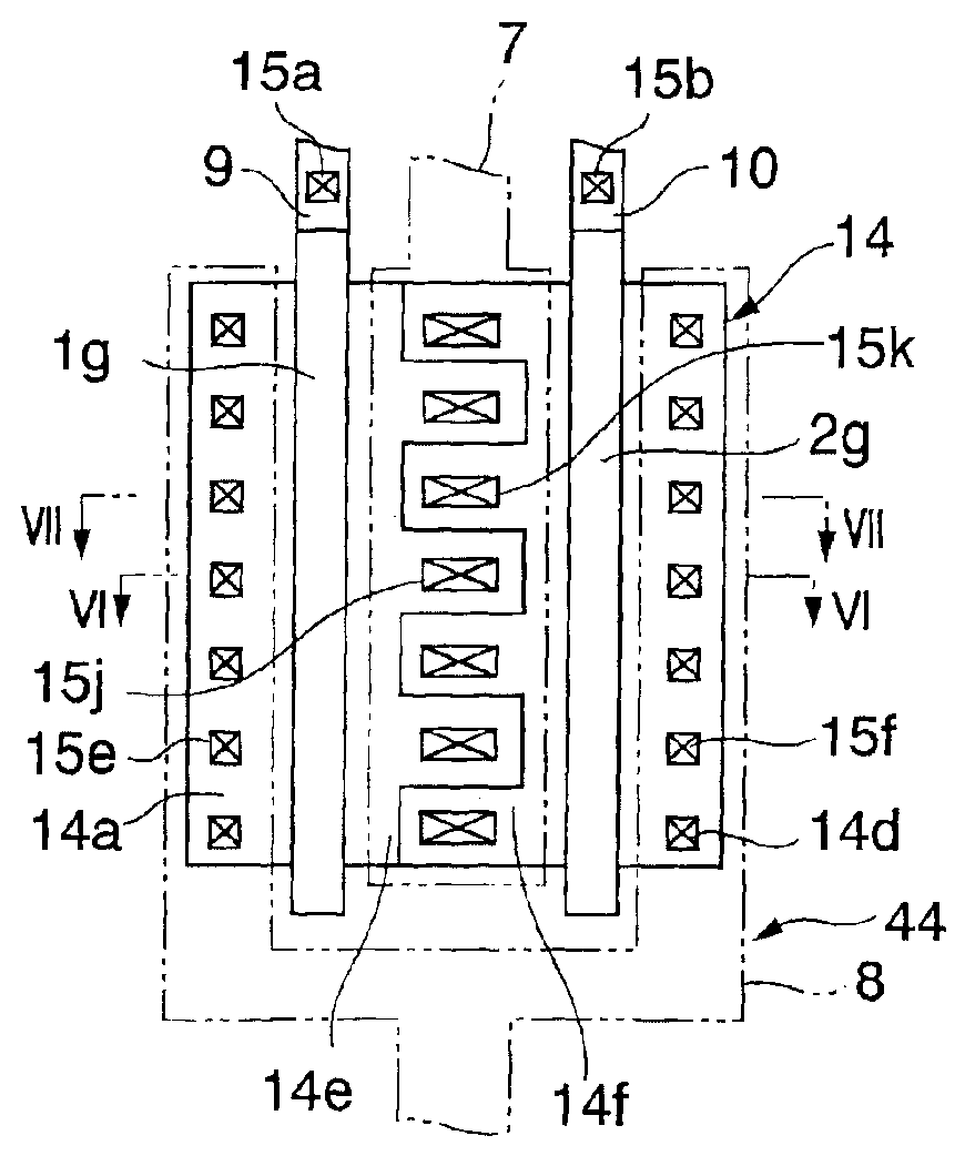
[0115]In a third embodiment, a CMOS analog switch having such a configuration that mutually neighboring source / drain regions of the p-channel thin film transistor and the n-channel thin film transistor are formed continuously not to leave a space between them and contact portions of the n-type source / drain and contact portions of the p-type source / drain are aligned on a straight line by arranging zigzag the boundary portions (joint portions) between neighboring n-type source / drain and p-type source / drain will be explained hereunder.

[0116]FIG. 11 is a plan view showing a layout of a CMOS analog switch according to the third embodiment of the present invention, FIG. 12A is a sectional view taken along a VI—VI line in FIG. 11, and FIG. 12B is a sectional view taken along a VII—VII line in FIG. 11. In FIG. 11 and FIG. 12, the same references as those in FIG. 5 and FIG. 6J denote the same elements.

[0117]In order to flow the large current, the polysilicon film 14 o...


PUM

PropertyMeasurementUnit
sizeaaaaaaaaaa
sizeaaaaaaaaaa
thicknessaaaaaaaaaa

Abstract

In a semiconductor circuit in a display device, there are provided a first gate electrode of a first MOS transistor formed on a semiconductor layer via a gate insulating film, a second gate electrode of a second MOS transistor formed on the semiconductor layer via the gate insulating film at a distance from the first gate electrode, first and second one conductivity type impurity introduced regions formed in the semiconductor layer on both sides of the first gate electrode to serve as source / drain of the first MOS transistor, and first and second opposite conductivity type impurity introduced regions formed in the semiconductor layer on both sides of the second gate electrode to serve as source / drain of the second MOS transistor. One of the first and second opposite conductivity type impurity introduced regions is formed to contact mutually to the second one conductivity type impurity introduced region.

Description

CROSS-REFERENCE TO RELATED APPLICATIONS[0001]This application is based upon and claims priority of Japanese Patent Application No. 2001-100395, filed in Mar. 30, 2001, the contents being incorporated herein by reference.BACKGROUND OF THE INVENTION[0002]1. Field of the Invention[0003]The present invention relates to a display device and a method of manufacturing the same and, more particularly, a display device in which a peripheral circuit or a signal processing circuit having the CMOS field effect transistor is built and a method of manufacturing the same.[0004]2. Description of the Prior Art[0005]In the active matrix liquid crystal display device in which the peripheral circuit or the signal processing circuit is built, the thin film transistors (TFTs) are employed as the CMOS transistors of the analog switch and the inverter in not only the display region but also the peripheral circuit or the signal processing circuit.[0006]The low-temperature polysilicon technology is utilized ...

Claims


Application Information

Patent Timeline
Patent Type & Authority Patents(United States)
IPC IPC(8): G02F1/13G02F1/1362G02F1/1368G09F9/00G09F9/30H01L27/08H01L29/786
CPCG02F1/136227H01L29/786
Inventor ZHANG, HONGYONGUCHIDA, NORIKO
Owner SHARP KK
Why Eureka
Try Eureka