Method for forming a conductive layer

a conductive layer and conductive technology, applied in the field of forming a conductive layer, can solve the problems of poor step coverage and voids, the difficulty of the etching step consequently increasing, and the inability to control the taper angle formed by the etching process to remain within the specification limits, so as to reduce the complexity of the etching process, and reduce the difficulty of the etching step.

Active Publication Date: 2005-08-02
IND TECH RES INST
View PDF7 Cites 92 Cited by
  • Summary
  • Abstract
  • Description
  • Claims
  • Application Information

AI Technical Summary

Benefits of technology

[0008]The object of the present invention is to provide a method for forming a conductive layer so that a deposited film with a taper is formed after a photolithography process. As a result, the step-coverage of a subsequently deposited multiplayer structure is improved, and the interlayer voids are minimized. Moreover, because the complex etchi...

Problems solved by technology

Unfortunately, the taper angle formed by etching process usually cannot be controlled sufficiently to remain within the specification limits.
However, the difficulty of the etching step is consequently increased.
Both the conditions mentioned above result in bad step coverage and occurrence of voids 250 during subsequent film deposition, ...

Method used


Image

  • Method for forming a conductive layer
  • Method for forming a conductive layer
  • Method for forming a conductive layer

Examples


example 1

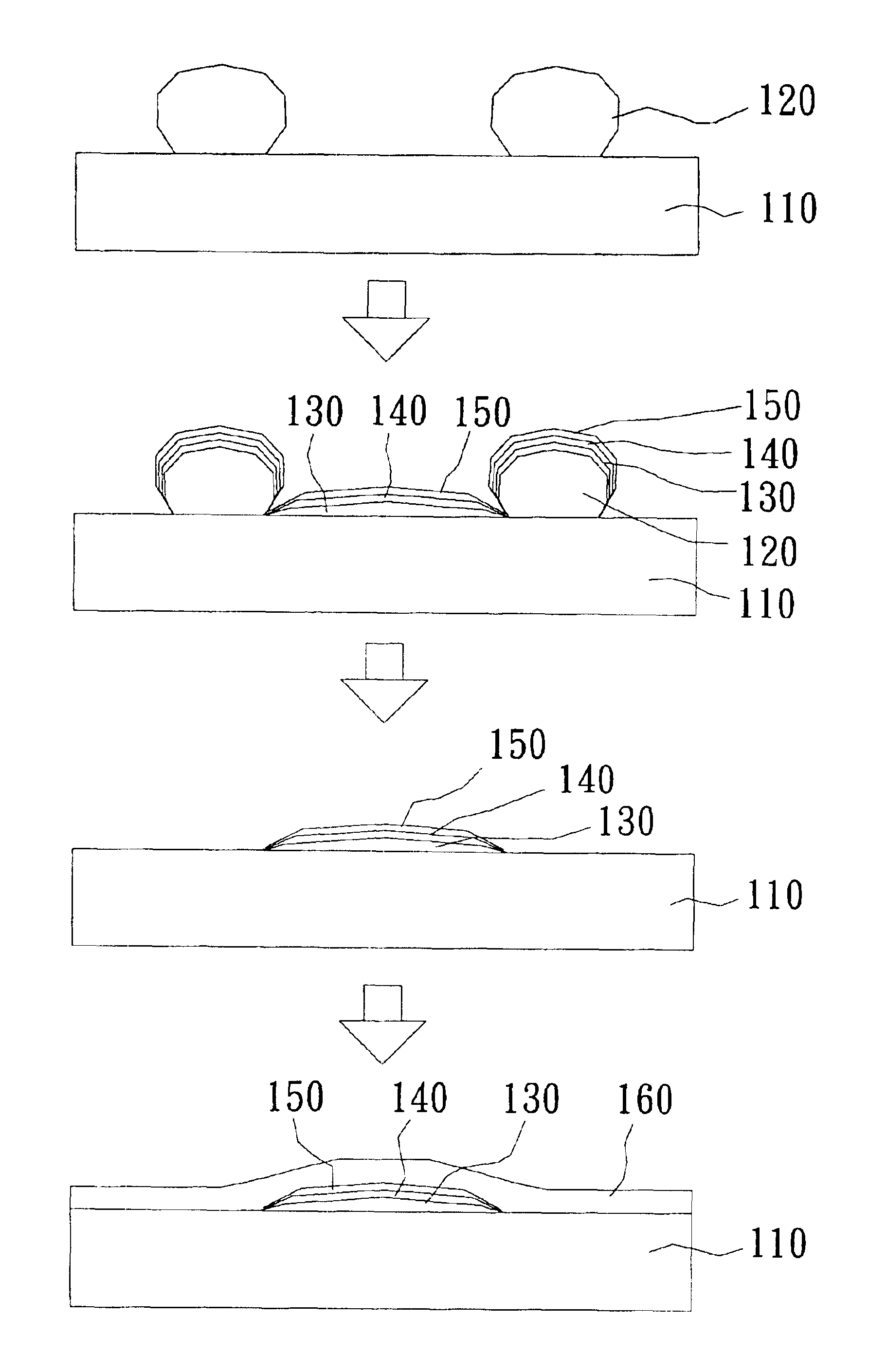
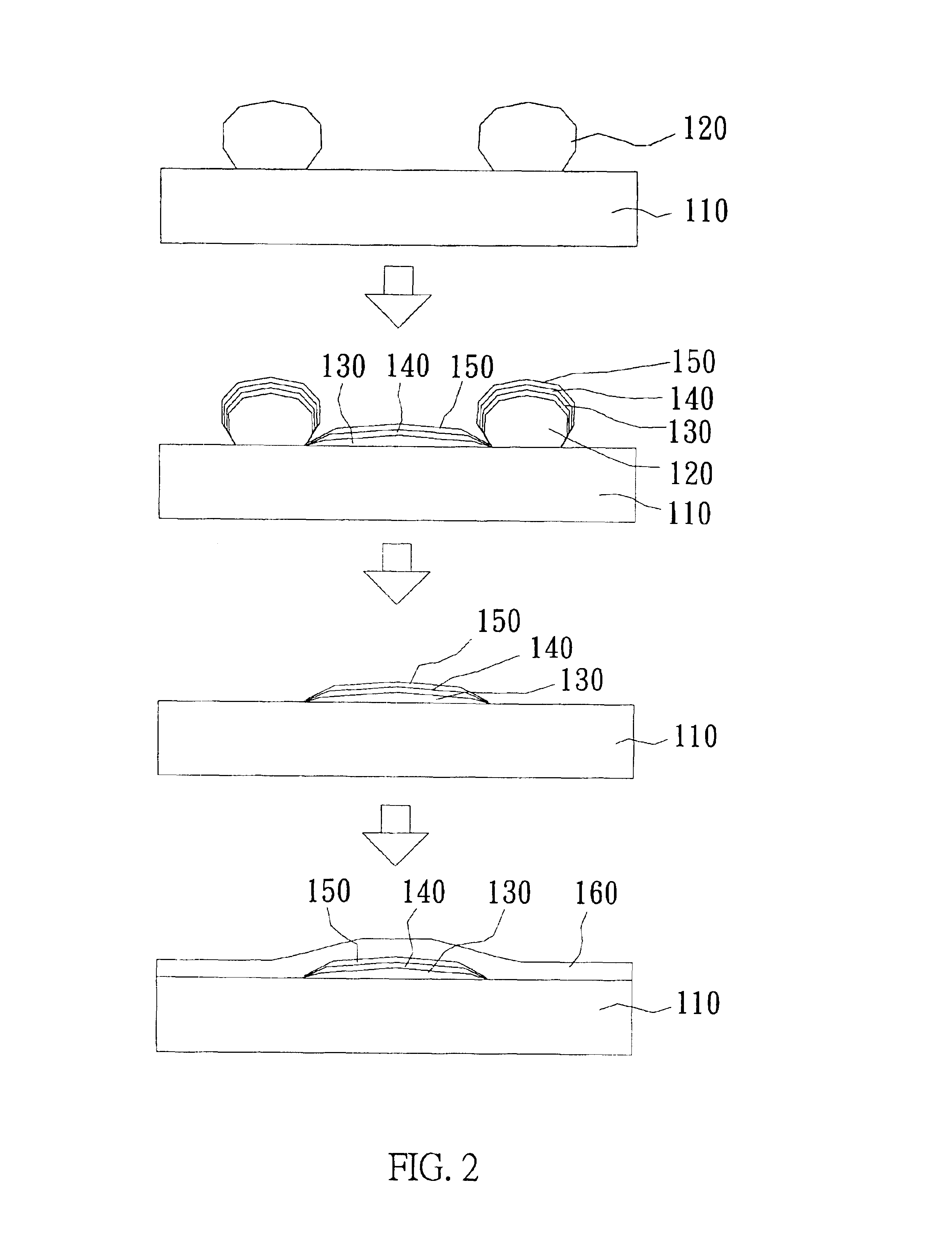
[0016]With reference to FIG. 2, there is shown a perspective view of the method of a preferred embodiment of the present invention. First, a substrate 110 is provided, wherein the surface of substrate 110 is made of glass, silica nitride, silica oxide, amorphous silicon, crystalline silicon, doped silicon, metals, metal nitrides, polymers, or organic light-emitting materials. Then, a photoresist layer is formed on the substrate 110, which is subsequently baked, exposed, and developed to form a patterned photoresist layer 120 thereon; wherein the parameters of the photolithography process, such as the thickness or composition of the photoresist, the energy of exposure, the depth of focus, the temperature of baking, or the time for developing are adjusted to form the patterned photoresist layer 120 having an undercut. Preferably, the patterned photoresist layer 120 has a cross section of a mushroom shape and is made of a negative photoresist. After that, a multilayer metal composed of...

example 2

[0018]With reference to FIG. 3, there is shown a perspective view of the method of another preferred embodiment of the present invention. With reference to FIG. 3, there is shown a perspective view of the method of another preferred embodiment of the present invention. First, a substrate 310 is provided, wherein the surface of substrate 310 is made of glass, silica nitride, silica oxide, amorphous silicon, crystalline silicon, doped silicon, metals, metal nitrides, polymers, or organic light-emitting materials. Then, a photoresist layer is formed on the substrate 310, which is subsequently baked, exposed, and developed to form a patterned photoresist layer 320 thereon; wherein the parameters of photolithography process, such as the thickness or composition of the photoresist, the energy of exposure, the depth of focus, the temperature of baking, or the time for developing are adjusted to form the patterned photoresist layer 320 having an undercut. Preferably, the patterned photoresi...


PUM

PropertyMeasurementUnit
Angleaaaaaaaaaa
Electrical conductoraaaaaaaaaa

Abstract

A method for forming a conductive layer is disclosed, which has the following steps. First, a substrate is provided, and then a patterned photoresist layer having an undercut is formed on the substrate. After that, at least one conductive layer is deposited on the substrate. Finally, the patterned photoresist layer is lifted off; wherein the shape of the conductive layer remaining on the substrate is complementary to that of the patterned photoresist layer.

Description

BACKGROUND OF THE INVENTION[0001]1. Field of the Invention[0002]The present invention relates to a method for forming a conductive layer and, more particularly, to a method for forming a gate electrode or a metal line of a transistor in manufacturing a thin film transistor liquid crystal display (TFT-LCD).[0003]2. Description of Related Art[0004]For the manufacturing of a thin film transistor array, it is critical to control well the taper angle of a film because the tapers may affect the step-coverage of subsequently deposited films, the formation of voids, and the yield of TFT-LCDs.[0005]The manufacturing of a TFT array mainly includes the steps of thin film deposition, photo-lithography, and etching, etc. for forming patterned conductive lines or gate electrodes. Currently, the taper angle is generally adjusted through regulating the parameters of the etching process, for example, use of particular etchant or gas to obtain a desired taper angle. Unfortunately, the taper angle for...

Claims


Application Information

Patent Timeline
IPC IPC(8): C23C16/06C23C14/06C23C14/14G02F1/13G03F7/26G02F1/1343G02F1/1345H01B13/00H01L21/28H01L29/786H01L21/4763H01L21/00H01L21/44H01L21/3205H01L21/02H01L29/66H01L21/027H01L21/336H01L29/49
CPCH01L21/0272H01L29/4908H01L29/66765Y10S438/952Y10S438/948
Inventor SUN, YU-CHANGTANG, CHING-HSUANLEE, CHI-SHENSHEU, CHAI-YUAN
Owner IND TECH RES INST
Why Eureka
Try Eureka