
Ultra-low latency multi-protocol optical routers for the next generation internet

a multi-protocol, optical router technology, applied in the field of interconnected computer networks, can solve the problems of limiting factors in scaling these large electronic routers, power requirements, and limiting factors in scalability of electronic routers, and achieve the effects of high data rate, low latency, and high throughpu

Inactive Publication Date: 2005-08-02
RGT UNIV OF CALIFORNIA
View PDF34 Cites 182 Cited by
  • Summary
  • Abstract
  • Description
  • Claims
  • Application Information

AI Technical Summary

Benefits of technology

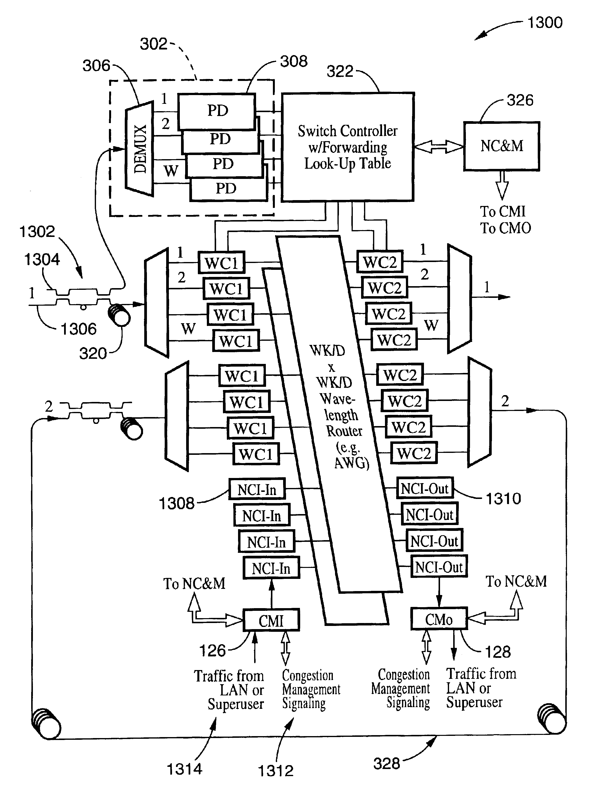
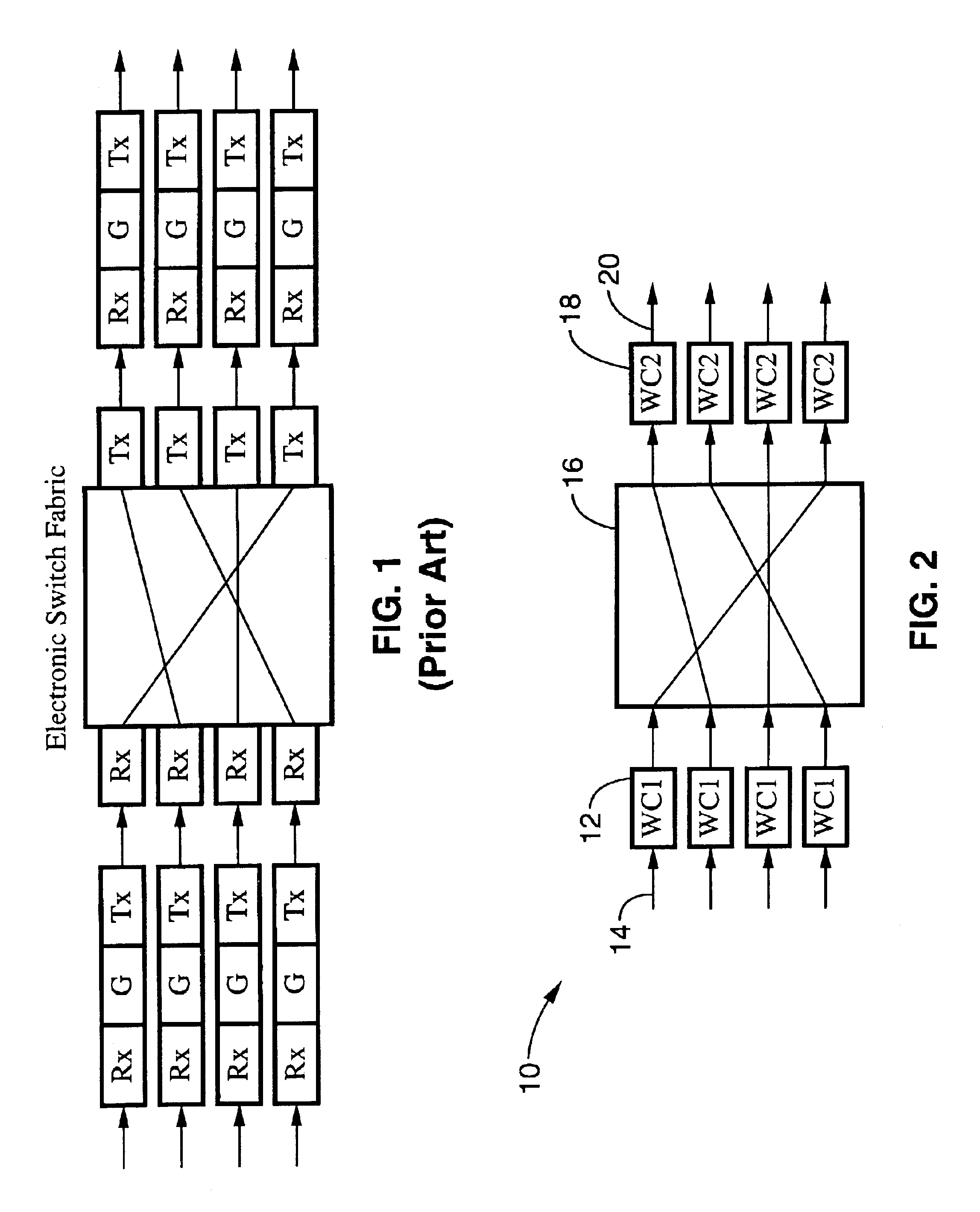
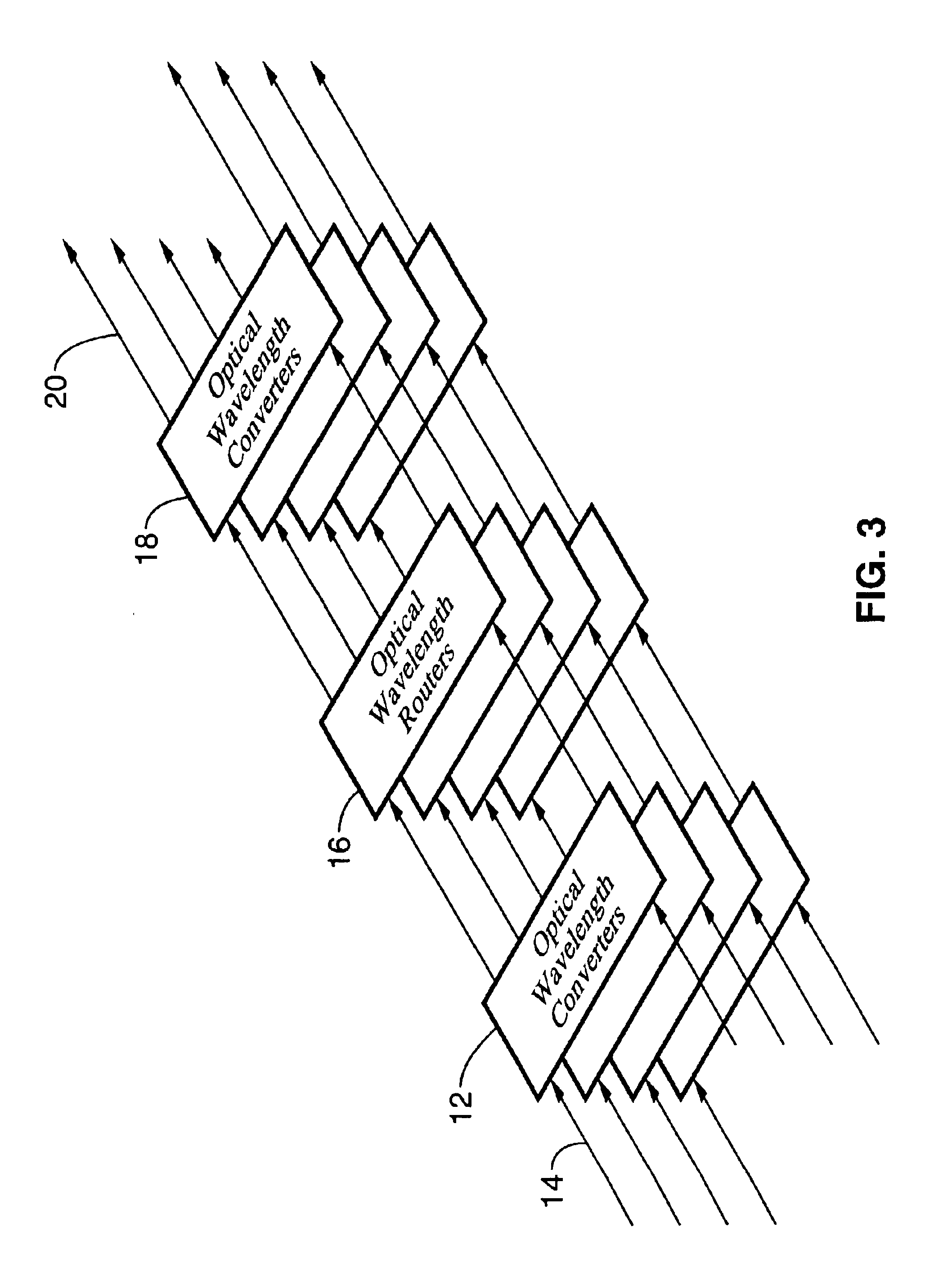
[0013]The inventive switching architecture utilizes well-established arrayed waveguide grating routers with wavelength converters at the edges. There is no active component at the core, and the number of active components at the edges scales as 2N where N is a product of the total number of ports and the total number of wavelengths. Hence, the power dissipation scales as 2a′N where a′ is the power dissipation of the optical wavelength converter to be discussed later. This is a significant improvement over electronic terabit switches which scale as 3aN+bN2, wherein a redundant number of transponders and transistors limit the scalability and performance due to power dissipation exceeding 10 kW for terabit routers.
[0015]The optical router also interfaces the local network to the Supernet, and adaptive congestion management will be achieved by early detection of network conditions. Constant communications and signaling linking the Supernet and local area networks (LANs) will be available with the present invention. The end users will benefit from high-throughput and minimum delay of the network realized by the optical router. Support of priority based class-of-service (CoS) and on-demand quality of service (QoS) will provide users with flexible and cost-effective utilization of the available network capacity.
[0022]Another object of the invention is to provide an optical router capable of routing packets with ultra-low latency and high throughput.
[0025]Another object of the invention is to provide an ultra-low latency, protocol-agile optical router that can potentially scale beyond 1024 by 1024 in connectivity and petabit per second switching capacity.

Problems solved by technology

While such routers demonstrate impressive aggregate switching capacities of terabits-per-second, however, it is evident that the power consumption and the physical size of these routers will limit scalability of the electronic routers much beyond the terabit regime.
One of the key limiting factors in scaling these large electronic routers lies in power requirements.

Method used


Image

  • Ultra-low latency multi-protocol optical routers for the next generation internet
  • Ultra-low latency multi-protocol optical routers for the next generation internet
  • Ultra-low latency multi-protocol optical routers for the next generation internet

Examples


example 1

[0104]Semiconductor, silica, and polymer based AWGs have been implemented to date. For InP based AWGs, the fabrication methods combine dry etching (e.g. reactive-ion-etching), wet chemical etching, and epitaxial regrowths (e.g. OMCVD). Rotation of the wafer during the epitaxial growths facilitates fabrication of uniform AWGs in order to reduce phase errors. In addition, it is possible to achieve three-dimensional integration of multiple of the inherently two-dimensional AWGs by adopting innovative lateral growth techniques offered by hydride vapor phase epitaxy (HVPE). This technique allows the first AWG to be fabricated and buried in an atomically planar surface. The second and subsequent AWG can be fabricated on the buried AWG.

[0105]FIG. 12A through FIG. 12H illustrate this fabrication procedure 700 of vertically integrating waveguide arrays. FIG. 12A illustrates the initial epitaxial growth of the InGaAsP waveguide core layer 702 on an InP substrate 704. FIG. 12B illustrates depo...


PUM


Abstract

An ultra-low latency optical router with a peta-bit-per-second total aggregate switching bandwidth, that will scale to a total connectivity of 1000 by 1000, and beyond by modular upgrades, that utilizes advanced optical technologies to achieve such high capacity with two to three orders of magnitude less volume and power requirements than the electrical router counter part, that serves as a universal engine to other optical routers being developed by vendors and researchers today, that can function in the context of circuit-switching, flow-switching, burst-switching, and packet-switching, that uses advanced wavelength conversion technology to effectively achieve three methods of contention resolution in the router: deflection in wavelength, deflection in space, and buffering in time, and that interfaces a local network to the Supernet.

Description

CROSS-REFERENCE TO RELATED APPLICATIONS[0001]This application is a continuation of U.S. application Ser. No. 09 / 654,384 filed on Sep. 1, 2000, now U.S. Pat. No. 6,519,062, which claims priority from U.S. provisional application Ser. No. 60 / 185,640 filed on Feb. 29, 2000, incorporated herein by reference.STATEMENT REGARDING FEDERALLY SPONSORED RESEARCH OR DEVELOPMENT[0002]Not ApplicableREFERENCE TO A MICROFICHE APPENDIX[0003]Not ApplicableNOTICE OF MATERIAL SUBJECT TO COPYRIGHT PROTECTION[0004]A portion of the material in this patent document is subject to copyright protection under the copyright laws of the United States and of other countries. The owner of the copyright rights has no objection to the facsimile reproduction by anyone of the patent document or the patent disclosure, as it appears in the United States Patent and Trademark Office file or records, but otherwise reserves all copyright rights whatsoever. The copyright owner does not hereby waive any of its rights to have ...

Claims


Application Information

Patent Timeline
Patent Type & Authority Patents(United States)
IPC IPC(8): H04Q11/00H04L12/56
CPCH04L45/00H04L45/50H04L45/52H04Q11/0005H04Q11/0066H04Q2011/0011H04Q2011/0016H04Q2011/0032H04Q2011/0073H04Q2011/0088
Inventor YOO, SUNG-JOO
Owner RGT UNIV OF CALIFORNIA
Learn More