

Proximity deposition
a technology of proximity and deposition, which is applied in the direction of solid-state diffusion coating, semiconductor/solid-state device testing/measurement, instruments, etc., can solve the problems of high difficulty, insufficient “clean” to cut the slice, and compromise the accuracy of cross-sectional analysis, etc., to achieve high secondary electron emission coefficient, high rate, and accurate measurement
- Summary
- Abstract
- Description
- Claims
- Application Information
AI Technical Summary
Benefits of technology
Problems solved by technology
Method used
Image

Examples
Embodiment Construction
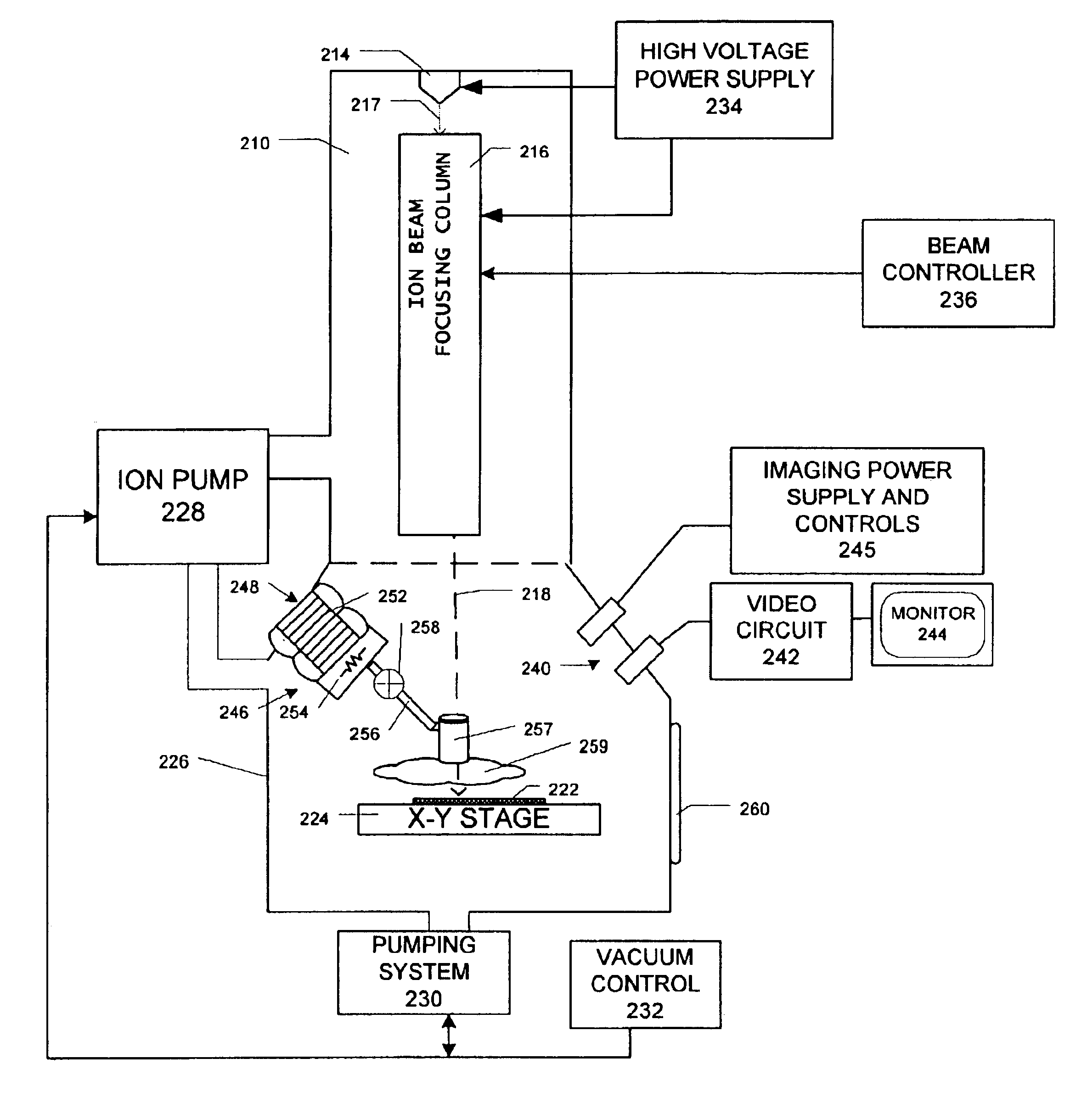
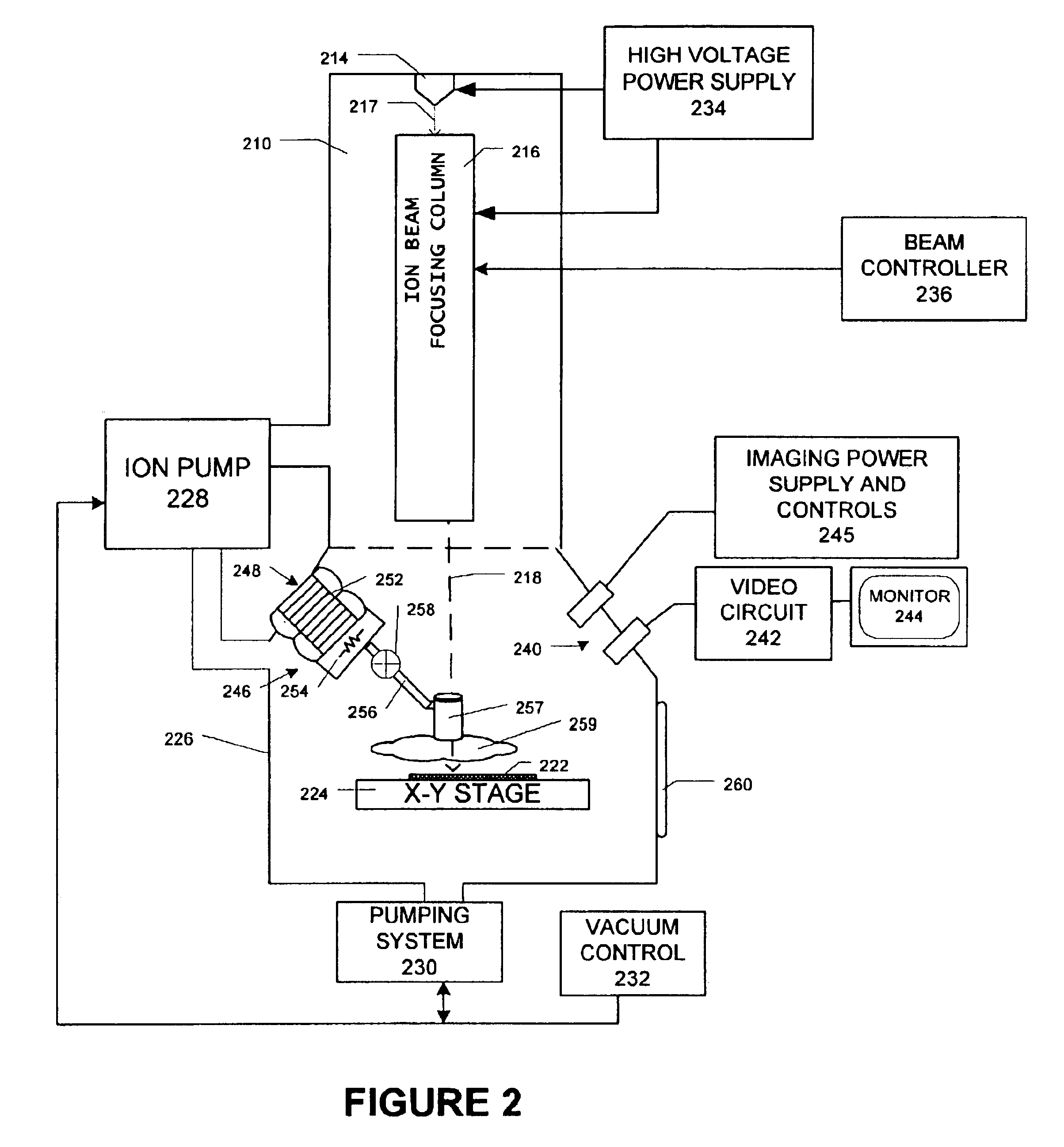
[0021]FIG. 2 schematically shows one embodiment of a focused ion beam (“FIB”) system suitable for practicing various embodiments of the proximity deposition method of the present invention. Note that the identified components are not required in all applications. Moreover, the depicted sizes and relative positions are not necessarily to scale or consistent with all configurations.
[0022]The depicted FIB system includes an evacuated chamber 210 having a liquid metal ion (e.g., Gallium) source 214 that generates ions 217 into a focusing column 216, which includes a conventional optical system having electrostatic lenses, electrodes (steering, deflection, etc.), and possibly other components for producing a desired focused ion beam 218 and focusing it onto a target work piece 222. Skilled persons will understand that the lenses and other “optical” elements used with focused ion beams use electrostatic or magnetic fields to control ions in the beam, and that the optical elements are cont...
PUM
| Property | Measurement | Unit |
|---|---|---|
| Area | aaaaa | aaaaa |
| Metallic bond | aaaaa | aaaaa |
Abstract
Description
Claims
Application Information