

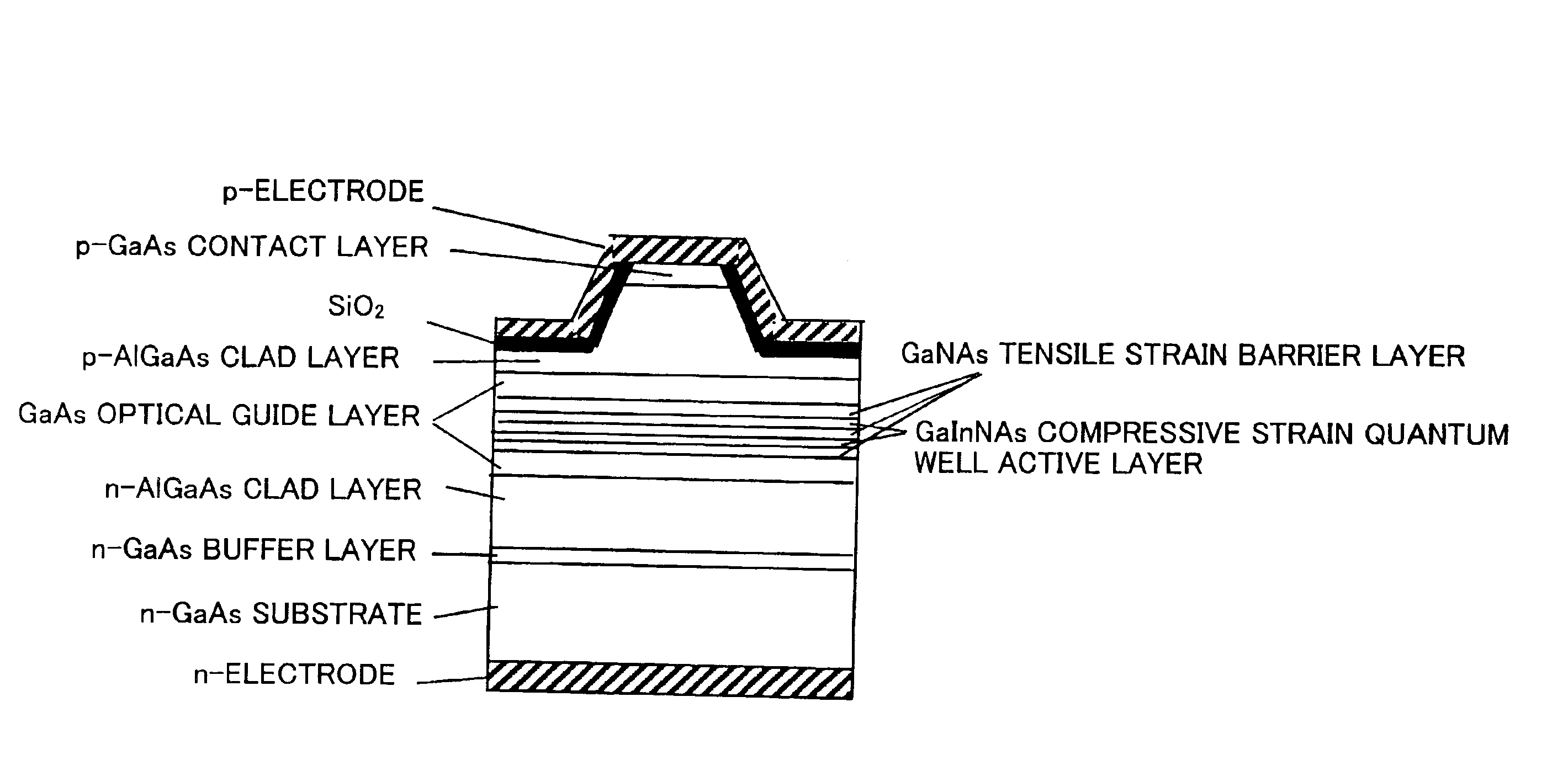
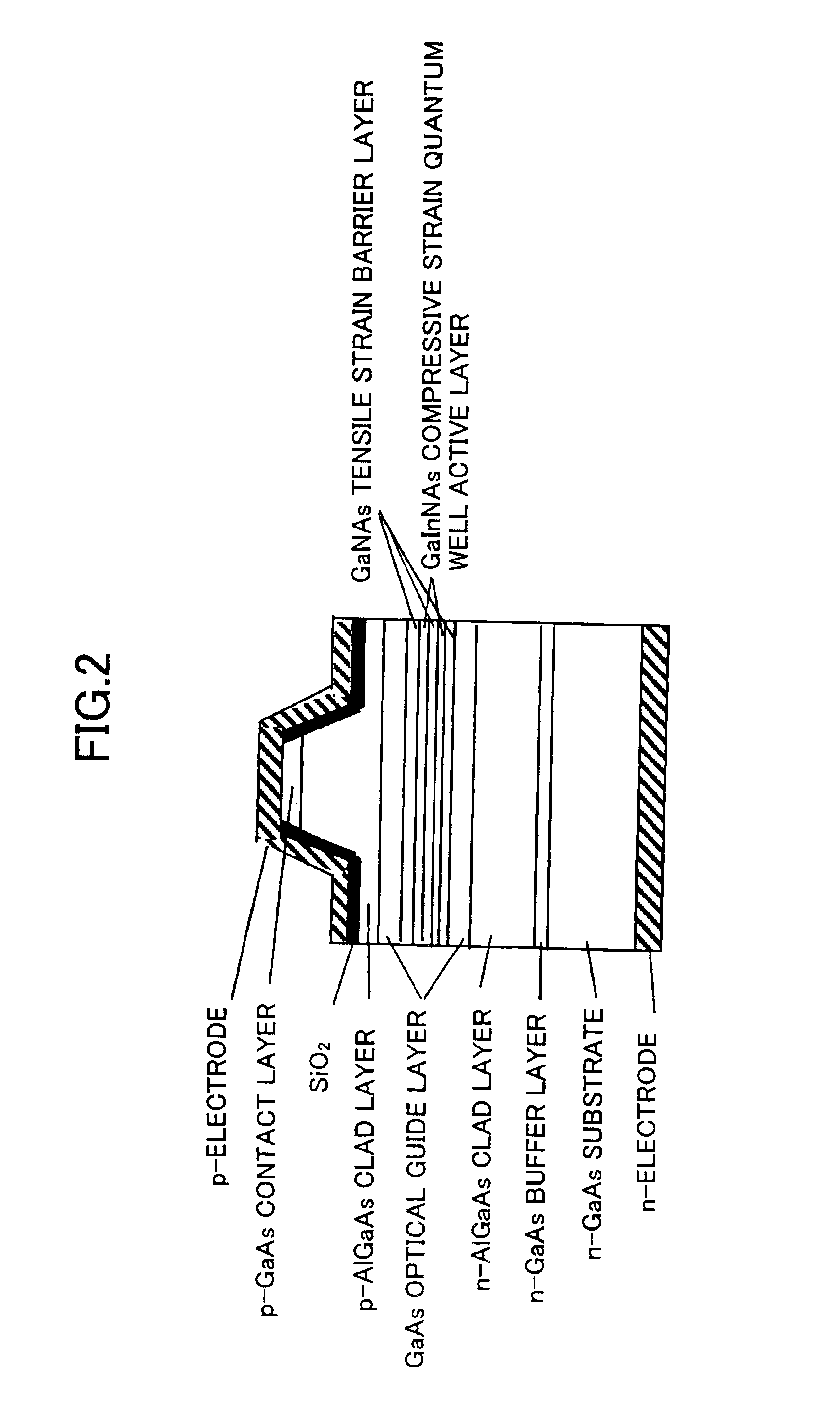
Semiconductor light emitter
a technology of semiconductors and light emitters, applied in the direction of semiconductor devices, lasers, semiconductor lasers, etc., can solve the problems of high current density, easy overflow of electrons, and rapid increase of threshold current density
- Summary
- Abstract
- Description
- Claims
- Application Information
AI Technical Summary
Benefits of technology
Problems solved by technology
Method used
Image

Examples
example 7
[0543]FIG. 43 is a drawing showing an optical transceiver module of a seventh example of the invention. The optical transceiver module of the seventh example is comprised of the surface emitting semiconductor laser of the third example, a photo-diode as a receiving end, and an optical fiber.
[0544]When the surface emitting semiconductor laser of the invention is used in an optical communication system, a highly-reliable optical communication system is provided at low costs by combining the surface emitting semiconductor laser (i.e., 1.3-micrometer-band GaInNAs surface emitting semiconductor laser), the photo-diode as a receiving end, and the optical fiber as shown in FIG. 43. Moreover, the surface emitting semiconductor laser using GaInNAs according to the invention is characterized by a satisfactory temperature characteristic, a low operating voltage, and a low threshold, thereby providing for a low cost system that emits less heat and is operable at high temperature without a cooli...
example 8
[0550]FIG. 44 is a drawing showing an active layer structure of a 1.3-micrometer-band surface emitting semiconductor laser according to the eighth example of the invention.
[0551]The eighth example differs from the third example in that GaNPAs is used for the barrier layer, and the quantum well active layer is comprised of GaInAsSb layers each being a 6-monoatomic layer and GaNAs layers each being a 2-monoatomic layer stacked one over the other 3.5 cycless in a short-cycle super lattice structure. The In composition of the GaInAsSb layer was 40%, and its Sb composition was 4%. The N composition of the GaNAs layer was 2%. Other compositions may suffice.
[0552]The quantum well active layer as described above has the GaInAsSb layers and GaNAs layers stacked one over the other with a thickness of each layer being a few atoms and without inclusion of both N and Sb at the same time and both In and N at the same time, and may thus be regarded as a material equivalent to a GaInNAsSb mixed cry...
example 5
[0632]FIG. 50 is a drawing showing an optical transmission module according to a fifth example of the invention. The optical transmission module of the fifth example is comprised of the surface emitting laser array chip of the fourth example combined with silica fibers. In the fifth example, laser light emitted by the surface emitting laser array chip is input into the optical fibers for transmission. The optical fiber is a single mode fiber in this example. In order to transmit a large amount of data simultaneously, parallel transmission is achieved based on the use of the laser array that is comprised of a plurality of integrated semiconductor lasers. The fifth example attains high-speed parallel transmission by use of single-mode high-power surface emitting lasers, thereby providing for an increased amount of data transmission compared with a conventional art.
[0633]Furthermore, the use of the surface emitting semiconductor lasers of the invention in an optical communication syste...
PUM
 Abstract
Description
Claims
Application Information