Process for manufacturing a semiconductor device

a semiconductor and manufacturing technology, applied in the field of semiconductor devices, can solve the problems of poor thickness uniformity in the plane of the substrate, low film depositing rate, and low ammonia gas flow rate, and achieve the effects of suppressing a semiconductor substrate, improving the thickness uniformity of the obtained silicon nitride film, and high film depositing ra

Inactive Publication Date: 2005-08-23
MITSUBISHI ELECTRIC CORP
View PDF9 Cites 5 Cited by
  • Summary
  • Abstract
  • Description
  • Claims
  • Application Information

AI Technical Summary

Benefits of technology

[0015]It is an object of the present invention to provide a high film depositing rate and to suppress a semiconductor substrate from being overheated in depositing a silicon nitride film.
[0016]It is ano

Problems solved by technology

(1) The ammonia gas of the source gases had to be supplied at a flow rate about 100 times the flow rate of silane gas. Since the ammonia gas is bad for the environment, the flow rate of ammonia gas must be reduced.
(2) The thickness uniformity of an obtained silicon nitride film in the plane of the substrate 51 is poor. For example, when a silicon substrate has a diameter of 10.16 cm (4 inches), the thickness uniformity in the plane is poor, i.e., about 13%.
(3) Since the thermal contact between the semiconductor substrate 51 and the substrate holder 52 is insufficient, the semiconductor substrate 51 is overheated by heat radiation

Method used


Image

  • Process for manufacturing a semiconductor device
  • Process for manufacturing a semiconductor device
  • Process for manufacturing a semiconductor device

Examples


first embodiment

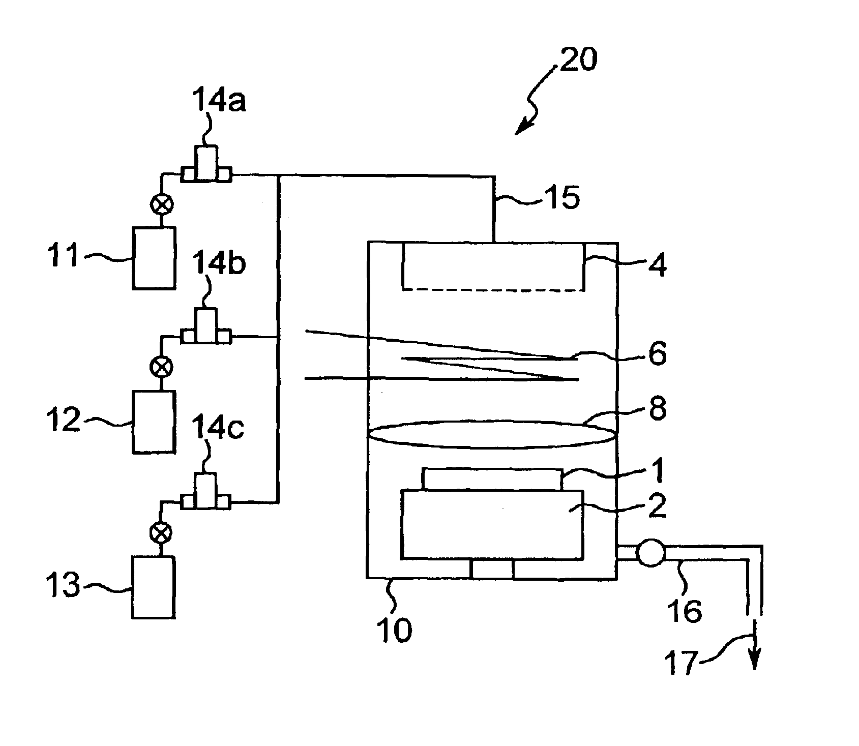
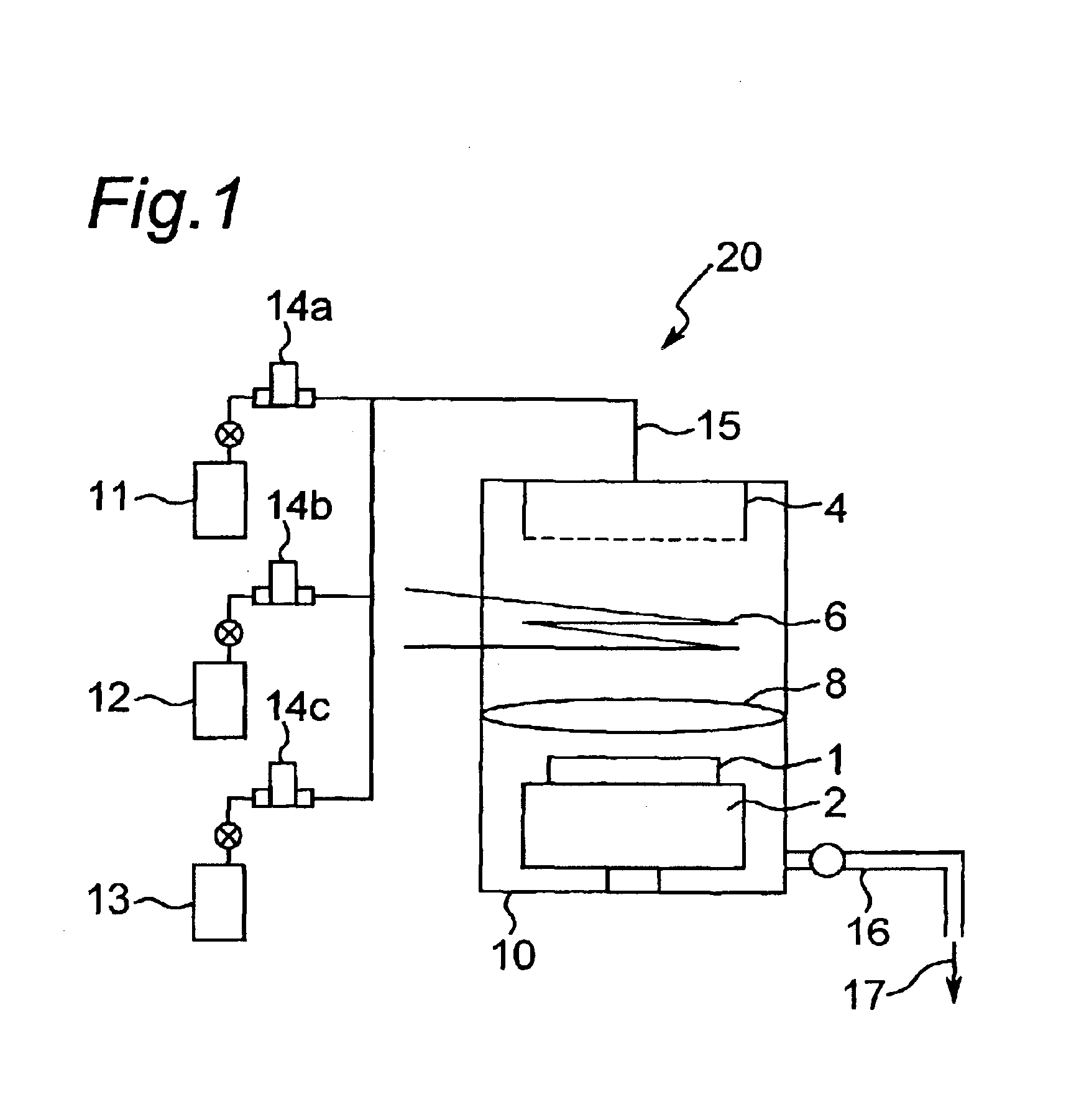
[0033]A process and apparatus depositing a silicon nitride film according to the present invention. The configuration of an apparatus 20 depositing this silicon nitride film will be described below with reference to the schematic view in FIG. 1. This film depositing apparatus 20 includes a reaction chamber 10 depositing a silicon nitride film on a semiconductor substrate 1 by catalytic CVD reaction process. This reaction chamber 10 includes a substrate holder 2 holding the semiconductor substrate 1, a gas supply unit 4 supplying source gases 5 containing a monosilane gas (SiH4), an ammonia gas (NH3), and a hydrogen gas (H2) onto the semiconductor substrate 1 in the reaction chamber 10, and a catalyzer 6 interposed between the gas supply unit 4 and the semiconductor substrate 1. The reaction chamber 10 may include a shutter 8 shutting out flows of the source gases from the gas supply unit 4 onto the semiconductor substrate 1. In addition, this film depositing apparatus 20 includes ga...

second embodiment

[0055]The process of depositing a silicon nitride film according to the present invention is shown in FIGS. 7 and 8. The temperature difference ΔT of the substrate 1 obtained by opening and closing the shutter 8 was 20° C. when a distance d1 between the catalyzer 6 and the semiconductor substrate 1 was 75 mm. When the distance d1 was 50 mm, the temperature difference ΔT was 28° C. As described above, even though the distance d1 between the catalyzer 6 and the semiconductor substrate 1 is 50 mm, the temperature difference ΔT can be suppressed to 50° C. or lower. Therefore, a film depositing rate could be increased to 9.5 nm / min.

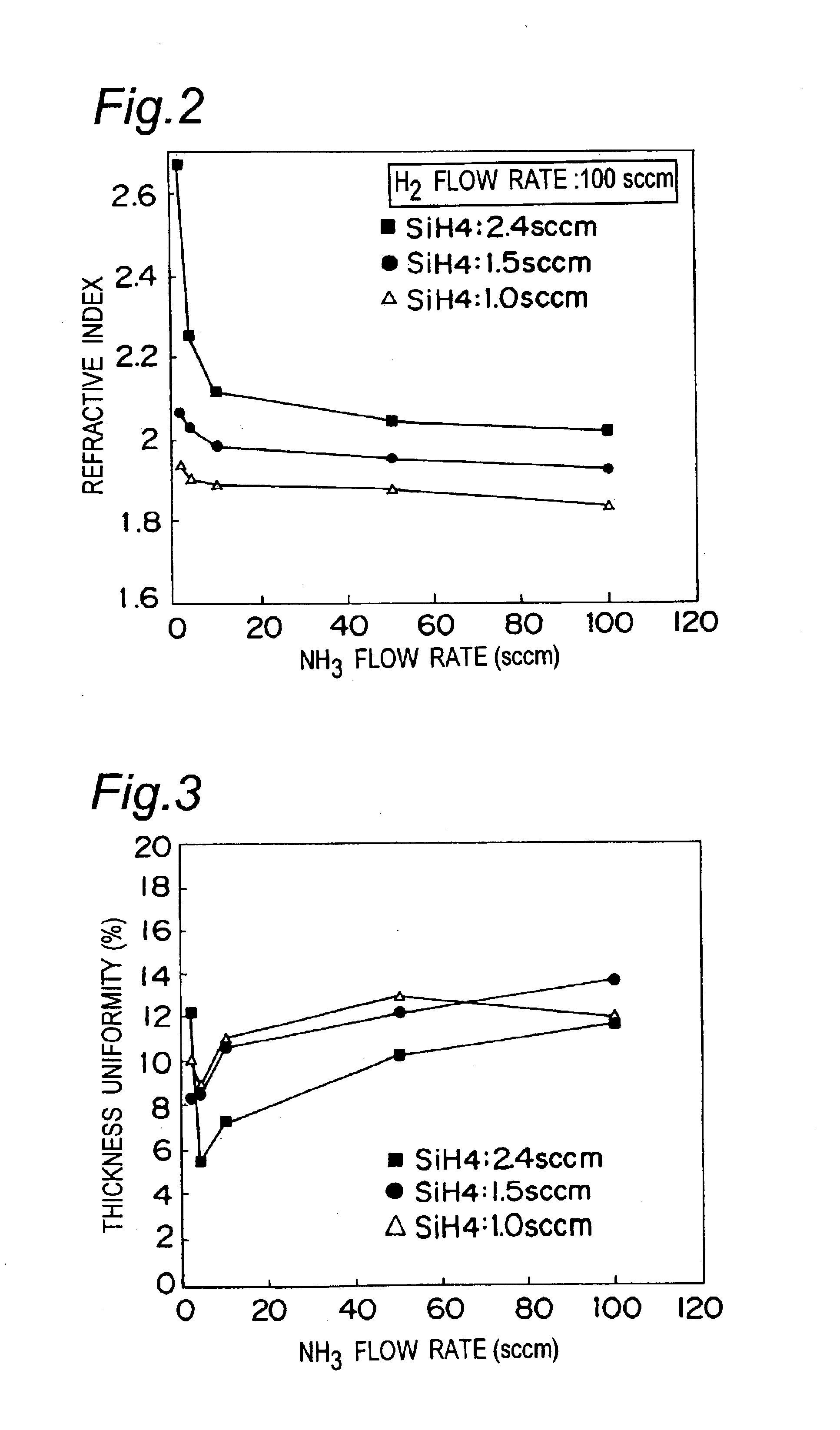
[0056]A process of depositing a silicon nitride film according to the third embodiment of the present invention will be described below. This process of depositing a silicon nitride film is different from the process of depositing a silicon nitride film according to the first embodiment in that flow rate of ammonia gas is reduced and that flow rate of hydrogen...


PUM


Abstract

A process of manufacturing a semiconductor device uses catalytic chemical vapor deposition. In the process, a reaction chamber containing a catalyzer and a substrate has gasses, including silane, ammonia, and hydrogen supplied to the reaction chamber. The gases are brought into contact with the catalyzer and then with the substrate to deposit a silicon nitride film.

Description

BACKGROUND OF THE INVENTION[0001]1. Field of the Invention[0002]The present invention relates to a semiconductor device having a silicon nitride film and, more particularly, to a semiconductor device having a silicon oxide film.[0003]2. Description of the Background Art[0004]As a process of depositing a silicon nitride film on a semiconductor substrate such as a silicon substrate, a process of nitriding the silicon substrate from its surface and a process of depositing a silicon nitride film by chemical vapor deposition (hereinafter referred to as CVD) are dominantly used. Of these processes, catalytic chemical vapor deposition (hereinafter referred to as catalytic CVD) is useful. In catalytic CVD, source gases including monosilane gas and ammonia gas are supplied through a heated catalyzer onto a silicon substrate to deposit a silicon nitride film onto the silicon substrate.[0005]Processes for depositing a silicon nitride film using this catalytic CVD will be described using FIG. 1...

Claims


Application Information

Patent Timeline
IPC IPC(8): C23C16/458C23C16/34C23C16/44H01L21/02H01L21/318C23C16/455H01L21/31
CPCC23C16/345C23C16/44C23C16/45512C23C16/4586C23C16/463H01L21/3185H01L21/02271H01L21/02211H01L21/0217H01L21/205
Inventor TOTSUKA, MASAHIROOKU, TOMOKIHATTORI, RYO
Owner MITSUBISHI ELECTRIC CORP
Why Eureka
Try Eureka