Optical techniques for measuring layer thicknesses and other surface characteristics of objects such as semiconductor wafers

a technology of optical techniques and surface characteristics, applied in the direction of manufacturing tools, lapping machines, instruments, etc., can solve the problems of significant amounts of undesired noise in the measurement signal, and achieve the effects of reducing the effects of scattering variations, reducing the source of noise, and increasing the depth of focus of the collection optics

Inactive Publication Date: 2005-08-23
LUMASENSE TECH HLDG
View PDF59 Cites 11 Cited by
  • Summary
  • Abstract
  • Description
  • Claims
  • Application Information

AI Technical Summary

Benefits of technology

[0011]The wide angle illumination and detection significantly reduces the effects of variations in scattering of the optical signals that can occur independently of the quantity desired to be measured. The incident optical radiation, and that modified by the surface being monitored, can be scattered varying amounts that depend upon the surface, angles that the radiation strikes the surface and optical elements, changes over time, and other causes. If the viewing angle is too narrow for a given angular extent of the illumination, for example, any variation in the amount of incident radiation that is scatted into the narrow viewing angle because of differences in scattering properties across the surface being monitored or between different surfaces, versus that which is scattered over wider angles out of view, causes the detected optical signal to vary. Significant variations can also occur when the surface is being viewed through a liquid layer, such as an etchant or slurry, that changes its thickness and other characteristics over time. These factors often cause the measurement signal to have significant amounts of undesired noise. But if the surface is illuminated and viewed over wide angles relative to that through which the incident radiation is scattered by the surface, any liquid etchant on it and by the optical elements, this source of noise is significantly reduced. It is reduced further when the surface is illuminated over wide angles. Illumination and detection over a full hemisphere is ideal but significant improvements are made when lesser angles in the range given above are utilized.
[0012]If a surface is illuminated with radiation over a very wide angle, such as 80 degrees or more, the surface modified radiation may be gathered for detection over a small angle, such as 25 or 15 degrees or less, and still provide the advantages described above. A small collection angle is often desired for other purposes, such as to increase the depth of focus of the collection optics, allow practical sized collection optics, increase the sensitivity of the measurement to the thickness of a films being monitored, in those applications, and / or to focus on a very small spot on the surface being monitored.
[0015]When the monitored layer is a metal or other generally opaque material, its reflectivity and emissivity are directly related to the thickness of the layer if the layer is thin enough to be at least partially transparent. For example, when a metal layer is being removed from a substrate, the layer's reflectivity or emissivity, when measured by the techniques summarized above, is directly related to the thickness of the metal layer once it has become thin enough to be semi-transparent. A metal film on a semiconductor wafer is semi-transparent when its thickness is less than about 500 to 1500 Angstroms, depending on the metal and the wavelength of radiation used. Therefore, for such thin metal layers, their thicknesses can be determined from a look-up table or set of functions that relate the measured reflectivity or emissivity with the layer's thickness. This makes it possible to measure and control the thicknesses of thin metal films with precision. Once the metal film is completely removed, then the optical properties being measured are those of the layers under the metal film. The measurement of the reflectivity or emissivity of a metal layer can be conducted with one or more wavelengths of optical radiation.
[0017]When two or more wavelengths of radiation are used to illuminate a layer, the radiation can be generated by separate narrow bandwidth radiation sources, such as light emitting diodes (LEDs), and then the uniquely responsive to one of the source wavelengths. Alternatively, or in combination, the two or more radiation sources are each modulated with a unique frequency. Electrical signals obtained from a single or multiple radiation receiving photodetectors are then filtered to pass the source modulating frequencies in order to obtain a separate signal for each of the illumination wavelengths. The frequencies of modulation are preferably selected to be different from that of any ambient radiation or electrical noise that might be present in the environment in which the measurements are being taken, thereby to significantly reduce adverse effects of any such ambient radiation and noise. The radiation source modulation and photodetector signal filtering technique can also be used when a single optical radiation is directed at the surface being monitored in order to similarly reduce the effects of any ambient radiation and electrical noise that might be present at different frequencies from the modulating frequency.

Problems solved by technology

These factors often cause the measurement signal to have significant amounts of undesired noise.

Method used


Image

  • Optical techniques for measuring layer thicknesses and other surface characteristics of objects such as semiconductor wafers
  • Optical techniques for measuring layer thicknesses and other surface characteristics of objects such as semiconductor wafers
  • Optical techniques for measuring layer thicknesses and other surface characteristics of objects such as semiconductor wafers

Examples


Embodiment Construction

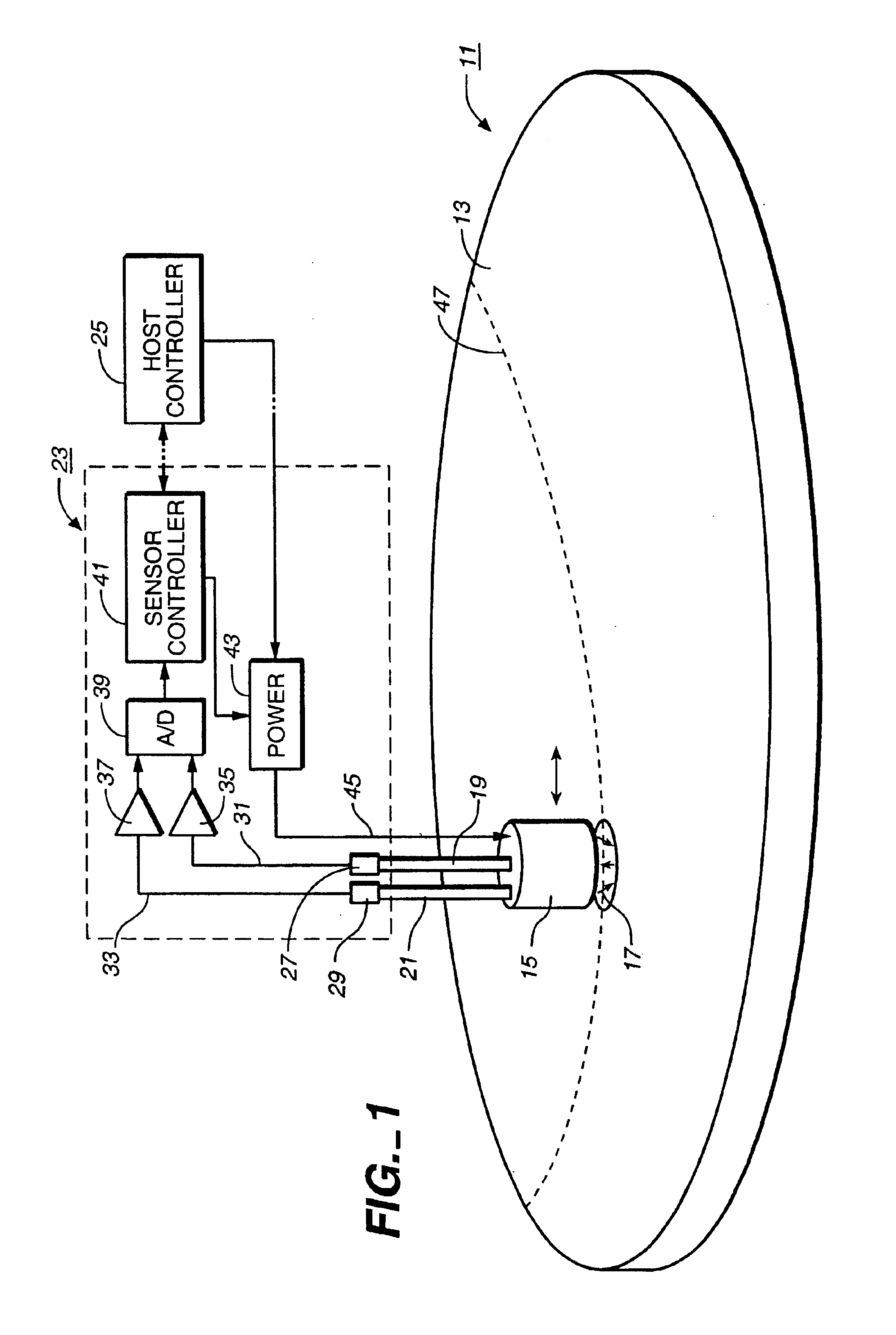
[0045]Referring initially to FIG. 1, a system utilizing the measurement techniques of the present invention is illustrated in general terms. A substrate or other object 11 contains a surface 13 that is being measured. An optical sensor head 15 directs optical radiation from one or more light emitting diodes (LEDs) against a spot 17 of the surface 13. Other sources of optical radiation can be used instead of LEDs but it is preferred that they have a narrow bandwidth, such as a few dozen nanometers in wavelength, or less. Highly coherent sources of optical radiation are unnecessary. A portion of the source radiation that is reflected from the surface is gathered by suitable optics, such as an optical fiber 19. Other optics, such as an optical fiber 21, collects a portion of the source radiation, preferably without any significant amount of radiation reflected from the surface, as background radiation that is used as a reference.

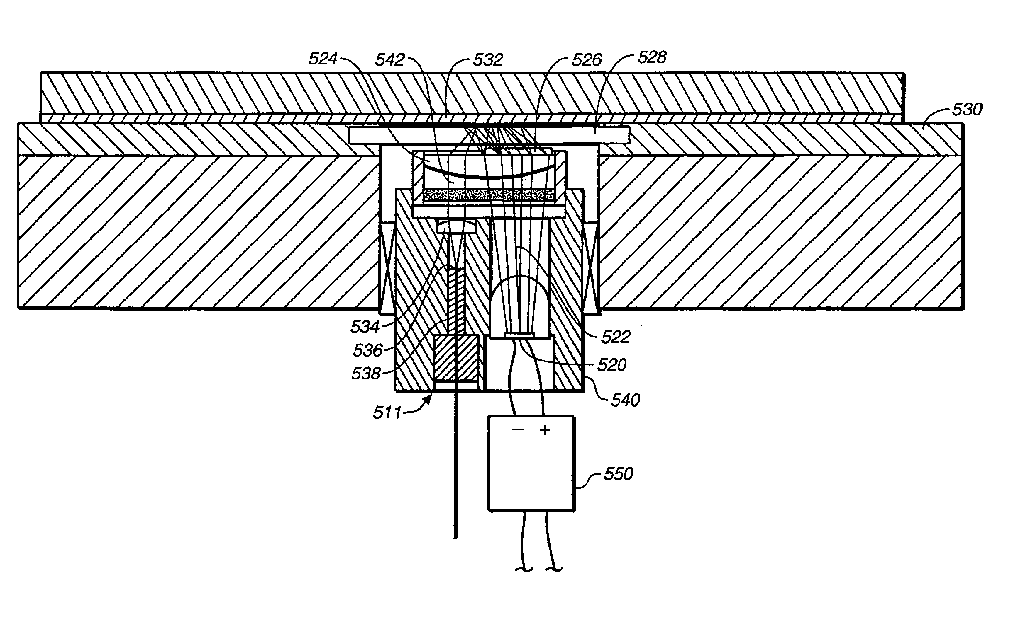
[0046]The sensor head 15 is connected with a module 23 th...


PUM

PropertyMeasurementUnit
angleaaaaaaaaaa
angleaaaaaaaaaa
angleaaaaaaaaaa

Abstract

A characteristic of a surface is measured by illuminating the surface with optical radiation over a wide angle and receiving radiation reflected from the surface over an angle that depends on the extend of the illumination angle. An emissivity measurement is made for the surface, and, alternatively, if a reflectivity measurement is made, it becomes more accurate. One application is to measure the thickness of a layer or layers, either a layer made of transparent material or a metal layer. A one or multiple wavelength technique allow very precise measurements of layer thickness. Noise from ambient radiation is minimized by modulating the radiation source at a frequency where such noise is a minimum or non-existent. The measurements may be made during processing of the surface in order to allow precise control of processing semiconductor wafers, flat panel displays, or other articles. A principal application is in situ monitoring of film thickness reduction by chemical-mechanical-polishing (CMP).

Description

CROSS-REFERENCE TO RELATED APPLICATIONS[0001]This application is a divisional of application Ser. No. 09 / 577,795, filed May 24, 2000, now U.S. Pat. No. 6,654,132 which in turn is a continuation-in-part of application Ser. No. 09 / 317,697, filed May 24, 1999, now U.S. Pat. No. 6,570,662 B1, which issued on May 27, 2003, which applications are incorporated herein in full by this reference.BACKGROUND OF THE INVENTION[0002]This invention relates generally to techniques for determining conditions of surfaces, and, more specifically, to doing so by measuring a characteristic of the reflectivity and / or emissivity of surfaces. An example application is the measurement of the thickness of a film on a substrate, such as a film that is formed or removed from a semiconductor wafer during the fabrication of integrated circuits. The thickness measurement is made either simultaneously with the film processing (in situ) or thereafter (in line). More specific applications include in situ measurements...

Claims


Application Information

Patent Timeline
Patent Type & Authority Patents(United States)
IPC IPC(8): B24B49/02B24B37/04B24B49/04B24B49/12G01B11/06G01N21/47B24B37/013
CPCB24B37/013B24B49/04B24B49/12G01B11/0625G01N21/4738
Inventor SCHIETINGER, CHARLES W.HOANG, ANH N.BAKIN, DMITRY V.
Owner LUMASENSE TECH HLDG
Why Eureka
Try Eureka