

Etch process for etching microstructures
a microstructure and etching technology, applied in the direction of instruments, optical elements, optical waveguide light guides, etc., can solve the problems of affecting the release of the final structure, requiring special equipment to handle, and collapsing of parts
Inactive Publication Date: 2005-08-30
APPLIED MATERIALS INC
View PDF11 Cites 28 Cited by
- Summary
- Abstract
- Description
- Claims
- Application Information
AI Technical Summary
Benefits of technology
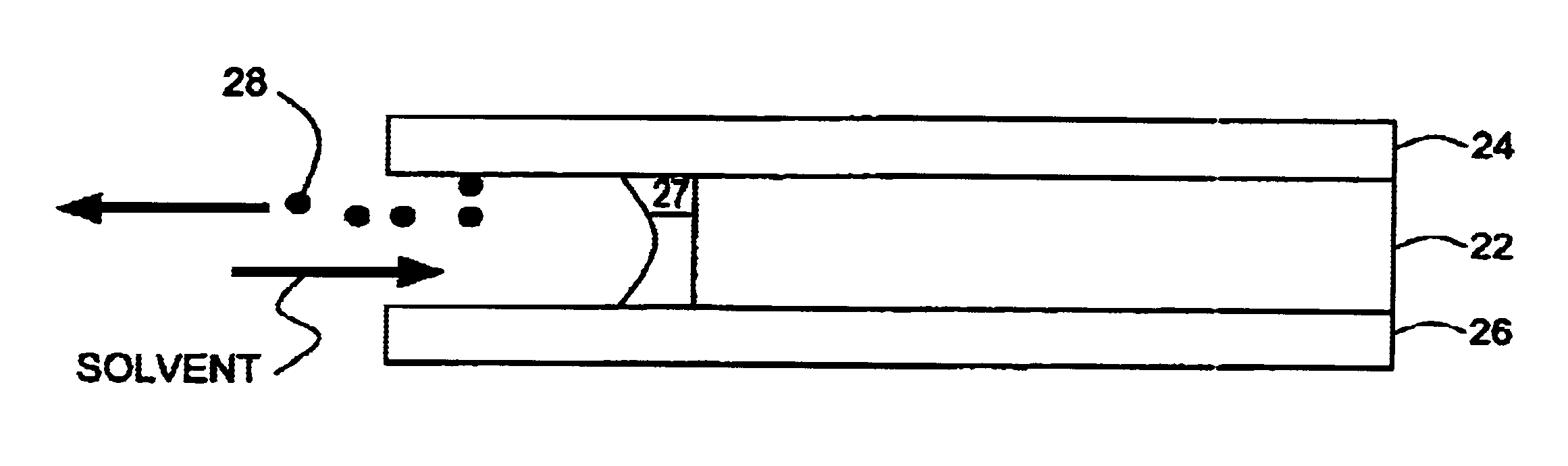
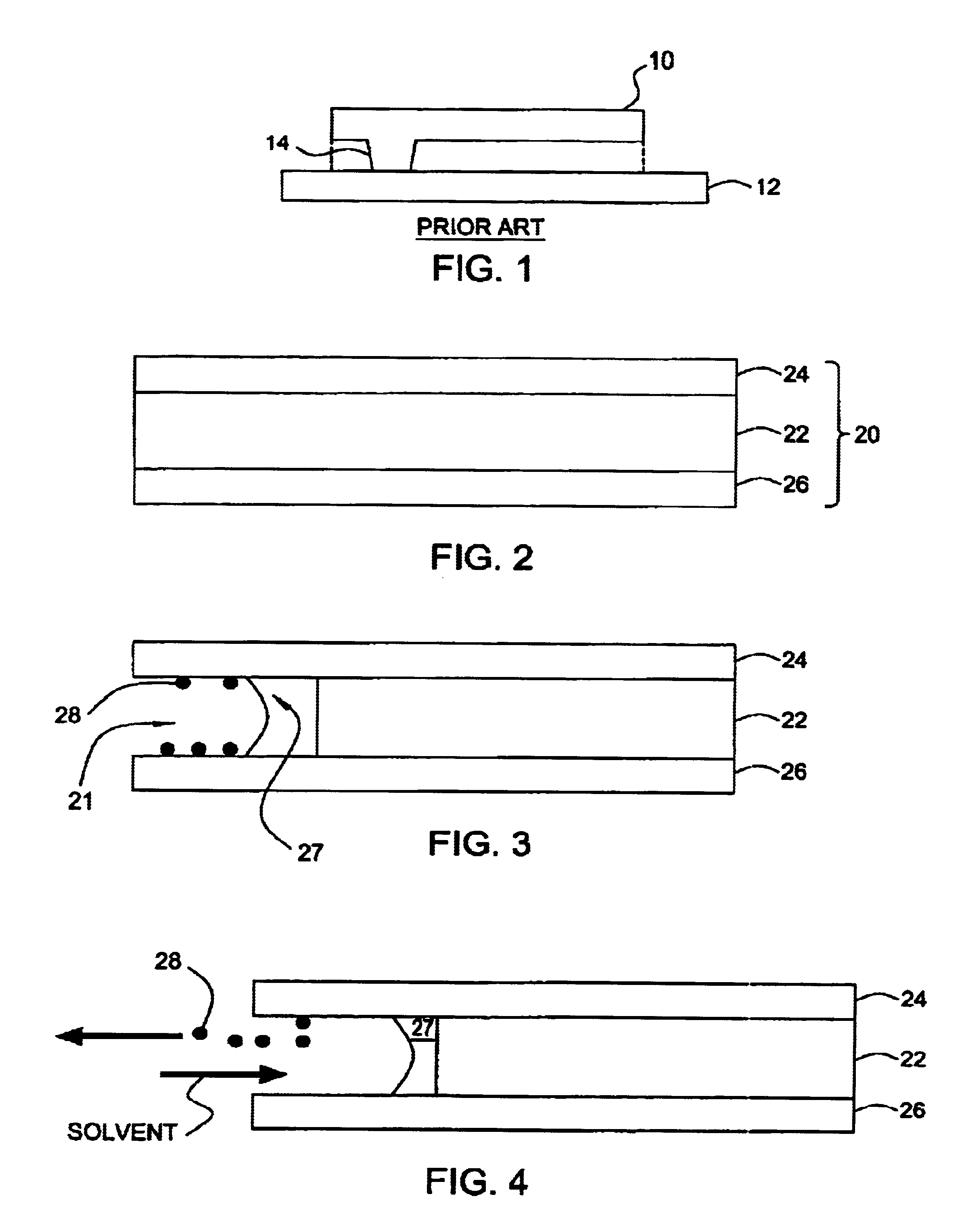
[0024]The first step uses a gaseous HF-H2O etchant mixture to etch a silicon oxide to form an opening between two silicon-containing layers. This step is continued for that amount of time sufficient to form structures that will not collapse during a subsequent drying step, but one that does not completely release the structure either. This first step does produce a residue however, as an excess of water is used to increase the etch rate of the silicon oxide to an acceptable level. Thus the timing for this first step is chosen to be such that the amount of etching is limited to that length of a device that cannot contact the underlying substrate during a subsequent step. Thus stiction is avoided by limiting the amount of etching that occurs during this first step.
Problems solved by technology
A major problem with processing such parts is that as etching proceeds, adherent residues form as by-products on the substrate, and capillary, van der Walls and electrostatic attraction between the etched part 10 and the substrate 12 causes collapse of the part 10.
In addition, etch by-products and contaminants in rinse waters also precipitate out of solution during drying steps, and cause adhesion bonding between the device part and the substrate that is even stronger than the electrostatic bonding, and interferes or prevents release of the final structure from the substrate.
However, because it is a very strong acid, special equipment is required to handle it.
Since other steps in the formation of MEMS devices use dry, rather than wet methods, and large multichamber units can be used to transfer a substrate from one processing step to another without requiring that the substrate be exposed to the atmosphere, it is undesirable to mix wet and dry processes when forming such devices.
The use of rinse solvents to remove moisture from a microstructure causes as many problems as it solves; the use of supercritical carbon dioxide requires a complex and difficult setup, and thus adds to the expense of manufacture.
Thus damage to the processing chamber occurs which must be repaired, adding to the cost of manufacture.
However, overall the etch rate of these oxides remains low.
This latter reaction does leave a residue which can cause stiction.
Further, the initial etching reaction also leaves a residue, and thus a rinse is necessary at completion of the anhydrous HF etch to remove the residue; this etch then is difficult to integrate into a multichamber or cluster tool that otherwise uses dry processes.
However, again, the etch rate is low initially until sufficient water is generated in the reaction, which leads to a low yield; further, the unknown initiation time hinders determination of the time required for release.
However, the etch rate here is low as well.
However, the etch rate is too low for commercial applications.
Thus the problem remains that by using anhydrous HF, the total time needed for release of a microstructure is long, and the etch rate cannot be known with certainty because it depends on the type of silicon oxide employed and the amount of water generated in the reaction.
Method used
View moreImage
Smart ImageViewing Examples

Examples
example
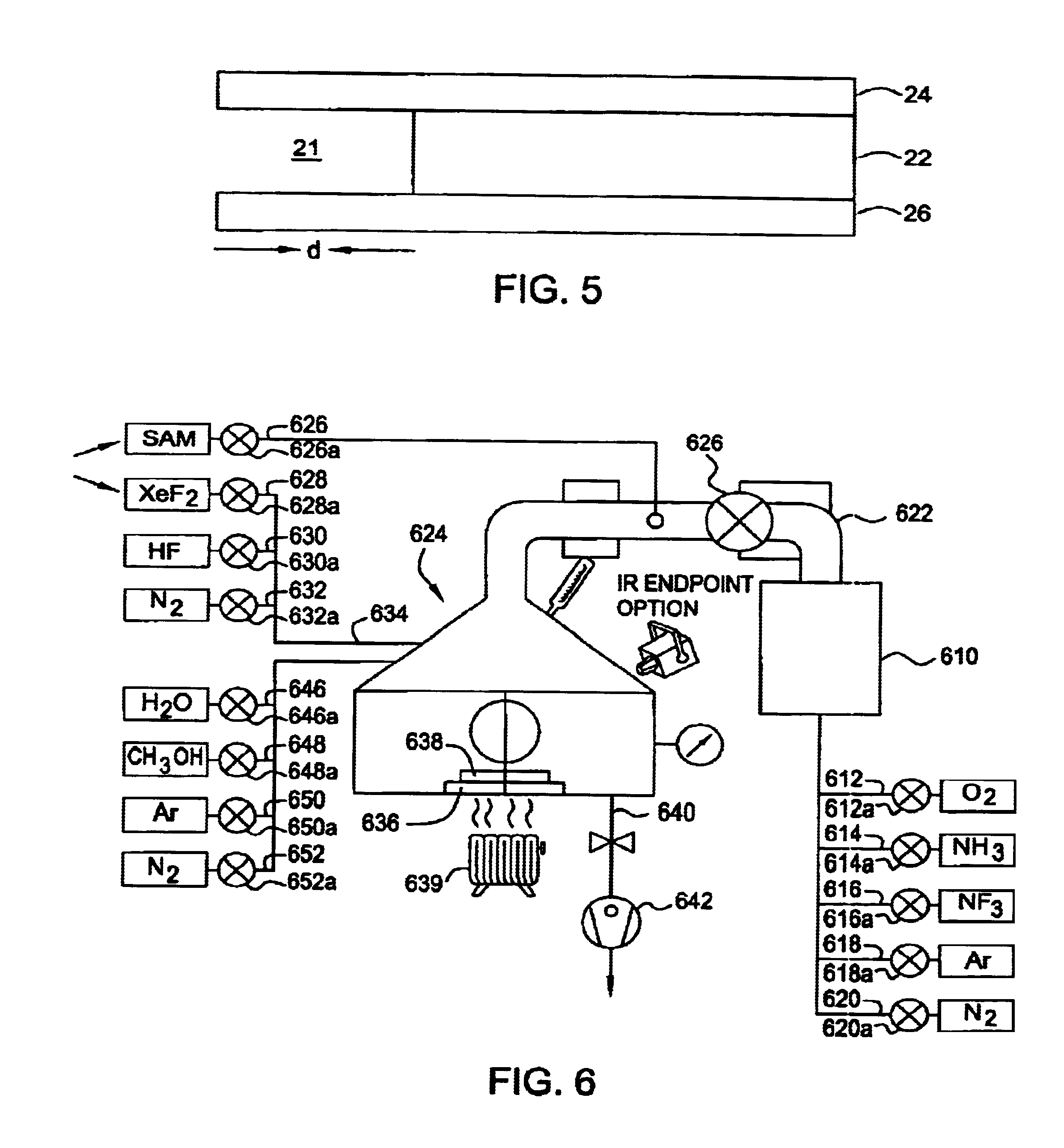
[0052]A layer of silicon dioxide deposited over a silicon layer and in turn having a polysilicon layer to be released deposited thereon, was etched using a mixture of 1.0 standard liters per minute (slm) of 5% by weight aqueous HF at a pressure of 100 millitorr and a temperature of about 40° C. to form a small opening in the silicon oxide layer. About 33 ml of liquid methanol were then added to the opening to dissolve any residue and rinse the opening.
[0053]The resultant opening was free of residues and methanol had replaced much of the water generated during etching.
[0054]These etch and rinse steps were repeated to form the desired device.
Login to View More PUM
| Property | Measurement | Unit |
|---|---|---|
| thickness | aaaaa | aaaaa |
| thickness | aaaaa | aaaaa |
| thickness | aaaaa | aaaaa |
Abstract
A two-step method of releasing microelectromechanical devices from a substrate is disclosed. The first step comprises isotropically etching a silicon oxide layer sandwiched between two silicon-containing layers with a gaseous hydrogen fluoride-water mixture, the overlying silicon layer to be separated from the underlying silicon layer or substrate for a time sufficient to form an opening but not to release the overlying layer, and the second step comprises adding a drying agent to substitute for moisture remaining in the opening and to dissolve away any residues in the opening that can cause stiction.
Description
[0001]This application claims the priority of Provisional Application No. 60 / 344,497 filed Oct. 17, 2001.[0002]This invention relates to a method of releasing microelectromechanical devices from a substrate using a gaseous etchant. More particularly, this invention relates to a method of releasing silicon-containing devices using a two-step method.BACKGROUND OF THE INVENTION[0003]Microelectromechanical systems (hereinafter MEMS) require controllable, partial separation of device parts from a substrate. Compliant silicon-containing microstructures are etched so as to completely release them from an underlying silicon-containing substrate. For example, an intermediate silicon oxide layer is etched to separate at least a portion of a silicon-containing layer from a substrate.[0004]A simple MEMS device is shown in FIG. 1. A device part, or beam 10, is partially isotropically etched from a substrate 12, leaving a support or connector 14 between them, that allows the part 10 to move, e.g....
Claims
Login to View More Application Information
Patent Timeline
 Patent Type & AuthorityPatents(United States)
IPC IPC(8): G02B6/36G02B6/122G02B6/12B81B3/00
CPCB81C1/00928G02B6/122B81C2201/112G02B6/3692G02B2006/12176
InventorCHINN, JEFFREY D.SOUKANE, SOFIANE
OwnerAPPLIED MATERIALS INC