Amplified photoconductive gate

a photoconductive gate and gate technology, applied in the field of terahertz photoconductive sampling of optical signals, can solve the problems of low signal to noise ratio, high limits of device sensitivity, and typical use of very slow scanning speed, and achieve low impedance, minimal rc time constant, and adequate signal to noise

Inactive Publication Date: 2005-08-30
LUNA INNOVATIONS
View PDF4 Cites 2 Cited by
  • Summary
  • Abstract
  • Description
  • Claims
  • Application Information

AI Technical Summary

Benefits of technology

[0010]Existing terahertz receivers are generally current amplifiers. Current amplifiers typically have low impedance and therefore a minimal RC time constant. However, they are typically used at very slow scanning speeds to achieve adequate signal to noise. When the illumination of the photoconductive region is well below saturation, or when a terahertz field is small, the amplifier noise current and any off-state noise current may be large in comparison to the actual current induced by the terahertz field. The mismatch in amplifier impedance with the off-state photoconductive device impedance may yield low signal to noise ratios. Current amplification can be used when the active area is strongly illuminated and slow scanning speeds are used. These amplifiers are also ideal for systems where stray capacitance is present and slow scan speeds are acceptable.
[0011]The current state of the art employs a photoconductive gate / antenna assembly simply as a current source for an external amplifier. Integration and signal averaging occur after the external amplifier. At low signal levels, the noise floor of a current amplifier is sufficiently high limits the sensitivity of the device. Moreover, because current amplifiers are not integral to the photoconductive gate / antenna assembly, the connecting wires increased the inherent capacitance in the system and adversely affected the response time of the assembly. As such, there is a need in the art for an integrated photoconductive gate and amplifier assembly in which the response time is optimized and the signal to noise ratio is maximized.
[0012]Accordingly, the present invention includes an amplified photoconductive gate having an integrated antenna and voltage amplifier. Voltage amplifiers can yield superior signal to noise because their input impedance can be large and match the large impedance of the photoconductive sampling gate. When the illumination of the gate is well below saturation, the large amplifier impedance allows the antenna amplifier circuit capacitance to reach equilibrium as driven by the repeated terahertz potential on the antenna during the sample gate. This multi-sample integration allows the antenna voltage to rise well above that of a single sample. Furthermore, by reducing the stray capacitance inherent in cabling, equilibrium can be reached in a minimal number of illuminations, thus allowing rapid scanning of the signal.
[0013]Voltage amplifiers can be integrated into a single housing with the photoconductive antenna. Integrating a low-input capacitance amplifier with the terahertz receiver increases sampling speeds, lowers the cost, and improves product robustness over the use of a typical current preamplifier. The signal-to-noise ratio achieved with voltage amplifiers is equal to or better than that achieved by systems employing current amplifiers, while still gaining all of the noted benefits.

Problems solved by technology

However, they are typically used at very slow scanning speeds to achieve adequate signal to noise.
The mismatch in amplifier impedance with the off-state photoconductive device impedance may yield low signal to noise ratios.
At low signal levels, the noise floor of a current amplifier is sufficiently high limits the sensitivity of the device.
Moreover, because current amplifiers are not integral to the photoconductive gate / antenna assembly, the connecting wires increased the inherent capacitance in the system and adversely affected the response time of the assembly.

Method used


Image

  • Amplified photoconductive gate
  • Amplified photoconductive gate
  • Amplified photoconductive gate

Examples


Embodiment Construction

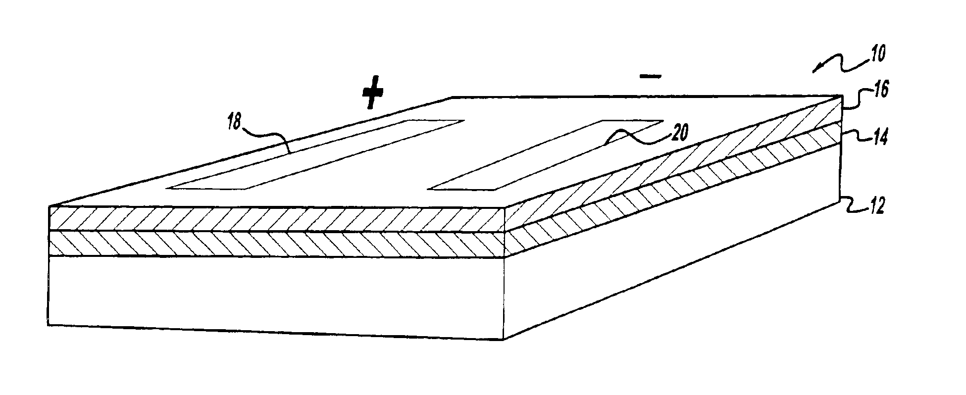
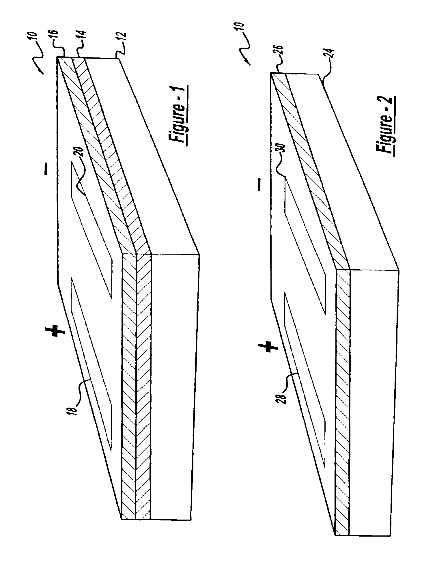
[0019]The present invention relates generally to the terahertz photoconductive sampling of optical signals utilizing a photoconductor and an associated amplifier. More particularly, the present invention relates to an optimized epitaxial photoconductive structure and associated voltage amplifier for such sampling, as discussed further herein.

[0020]FIG. 1 is a diagrammatic illustration of a terahertz photoconductive semiconductor epitaxial structure having a barrier layer, termed a photoconductive gate 10. The photoconductive gate 10 includes a substrate 12 composed of GaAs. A barrier layer 14 is disposed between the substrate 12 and the photoconductive layer 16. A bipolar terahertz antenna comprised of a first pole 18 and a second pole 20 is disposed on the photoconductive layer 16. Although the first pole 18 is designated positive and the second pole 20 is designated negative, it is understood that the respective charges of the poles of the terahertz antenna may be reversed.

[0021]A...


PUM


Abstract

The present invention includes a semiconductor epitaxial structure optimized for photoconductive free space terahertz generation and detection; and amplifier circuits for photoconductively sampled terahertz detection which may employ the optimized epitaxial structures.

Description

CROSS-REFERENCE TO RELATED APPLICATIONS[0001]The present application claims priority to U.S. application No. 60 / 334,549, filed Nov. 29, 2001.FIELD OF THE INVENTION[0002]The present invention relates generally to the terahertz photoconductive sampling of optical signals, and more particularly to an optimized epitaxial photoconductive structure and associated voltage amplifier for such sampling.BACKGROUND AND SUMMARY OF THE INVENTION[0003]Epitaxial structures of low temperature grown gallium arsenide (GaAs) photoconductive devices can be tailored to the specific and differing needs of both free-space terahertz generation and free-space terahertz sampling. Low temperature GaAs can also be grown as a heterostructure with a tailored growth profile. When grown at approximately 600° C., GaAs has a recombination rate on the order of 1 nanosecond. Under these conditions, the strucutre is its natural or stoichiometric state, and has equal quantities of Ga and As forming the lattice.[0004]It i...

Claims


Application Information

Patent Timeline
Patent Type & Authority Patents(United States)
IPC IPC(8): G01J5/20H01L31/06H01L31/062H01L31/101H01L31/113H01L31/112H01Q23/00
CPCH01L31/09H01Q23/00H01S1/02H03F3/087H03F3/45475H03F17/00H03F2203/45138
Inventor WILLIAMSON, STEVEN L.RUDD, JAMES V.ZIMDARS, DAVIDWARMUTH, MATTHEWCHERNOVSKY, ARTUR
Owner LUNA INNOVATIONS
Why Eureka
Try Eureka