
Optical module for high-speed bidirectional transceiver

a bidirectional transceiver and optical module technology, applied in the field of optical modules for high-speed bidirectional transceivers, can solve the problems of reducing the overall performance of the station, requiring many expensive and time-consuming adjustments, and cumbersome arrangement in implementation, so as to simplify the adjustment procedure

Inactive Publication Date: 2005-09-06
MICROALIGN TECH +1
View PDF19 Cites 100 Cited by
  • Summary
  • Abstract
  • Description
  • Claims
  • Application Information

AI Technical Summary

Benefits of technology

[0019]It is an object of the present invention to provide an optical module for a high-speed bidirectional transceiver which is simple in construction, inexpensive to manufacture, facilitates optical alignment of the optical components during assembling and therefore is suitable for mass production, utilizes short lead wires that results in low inductivity of the device, can be mounted on a PC board and matched with its circuitry, and allows, in combination with respective electronics, to reach data transmission speeds exceeding 1 Ggbit / sec.SUMMARY OF THE INVENTION

Problems solved by technology

Although simple in theory, such an arrangement is cumbersome in implementation.
Such coupling requires many expensive and time-consuming adjustments to achieve optimum alignment.
Additionally, the optical losses attributed to this coupling, including attachment between the duplexer, fiber, transmitter and receiver, may degrade the overall performance of the station to an unacceptable level.
Further, Weidel is necessarily limited to providing coupling between both a transmitter and receiver to an optical fiber.
However, there exist situations wherein a pair of transmitters, operating at different wavelengths, must be coupled over the same fiber (unidirectional transmitter).
However, a main disadvantage of the device disclosed in U.S. Pat. No. 4,904,043 consists in that a photoreceiver should always be optically coaxial with an optical axis of one of two light sources that generate light of a working wavelength λ1 or λ2.
Such a design is inconvenient for suppression of crosstalk, e.g., a parasitic signal with the wavelength λ2 when a photodiode receives a useful signal with wavelength λ1.
One disadvantage of the transceiver of U.S. Pat. No. 5,485,538 consists in that all optical elements, including HOE, used for beam management transform the beams into converging or diverging beams.
This creates significant problems for alignment of the beams because all the optical elements must be adjusted simultaneously.
Another disadvantage, which is inherent in all orthogonal bidirectional transceivers, consists in that their geometry is unsuitable for use in conjunction with high-speed controllers.
Therefore the device of this patent entails all disadvantages of the previously described design, including speed limitations due to geometry.
Although the bidirectional transceiver of U.S. Pat. No. 5,621,573 partially simplifies the alignment procedure due to the use of preassembled units, the limitations by speed remain unsolved due to the use of practically the same geometry as in all previously known orthogonal arrangements.
A disadvantage common to all four last-mentioned patents of Lucent Technologies Inc., as well to all preceding structures, is that the orthogonal geometry used in the bidirectional optical transceivers described in the aforementioned patents make it difficult to use such devices in high-speed systems with frequencies of 500 MHz or higher.
This limitation restricts the speed of transmission data through the bidirectional transceiver.

Method used


Image

  • Optical module for high-speed bidirectional transceiver
  • Optical module for high-speed bidirectional transceiver
  • Optical module for high-speed bidirectional transceiver

Examples


Embodiment Construction

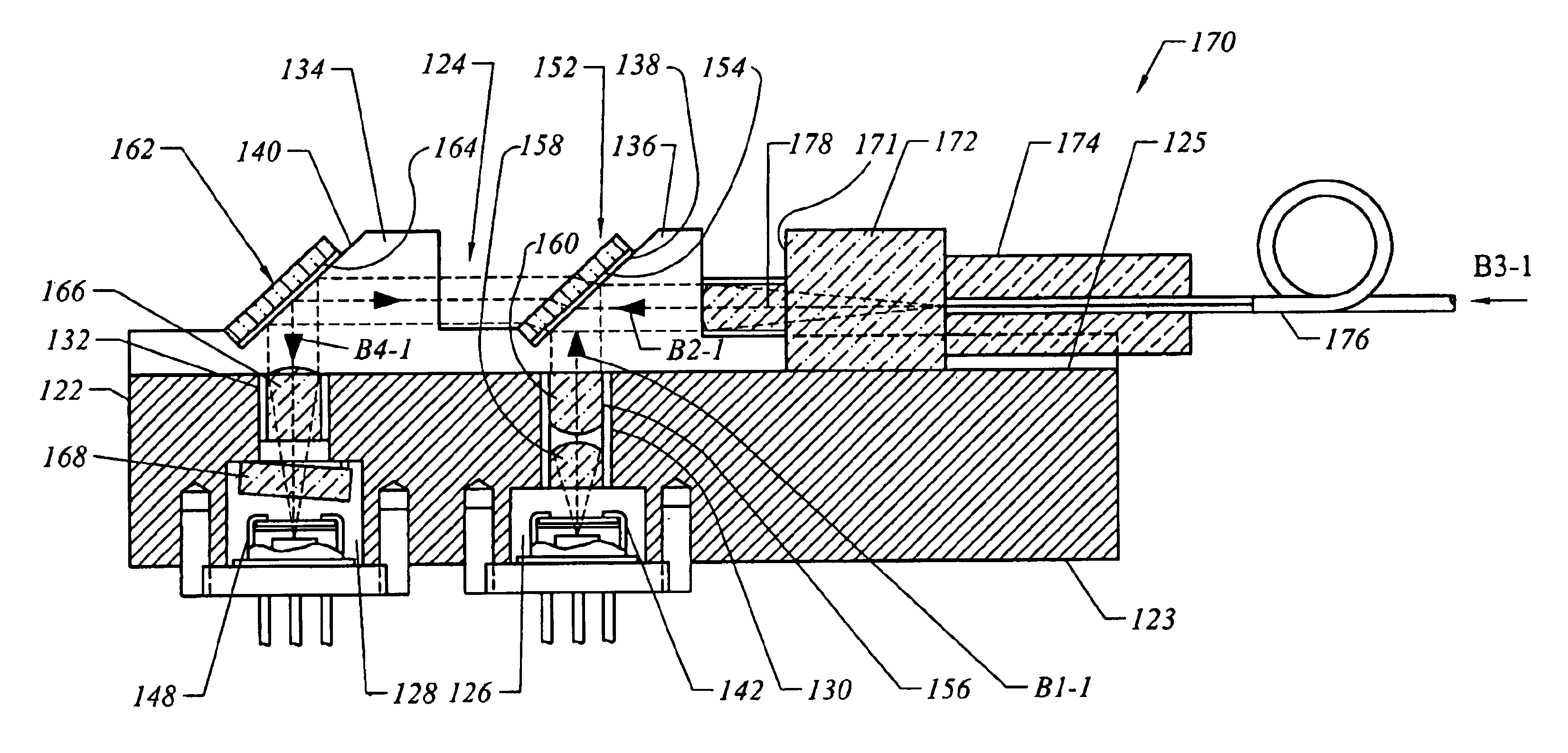
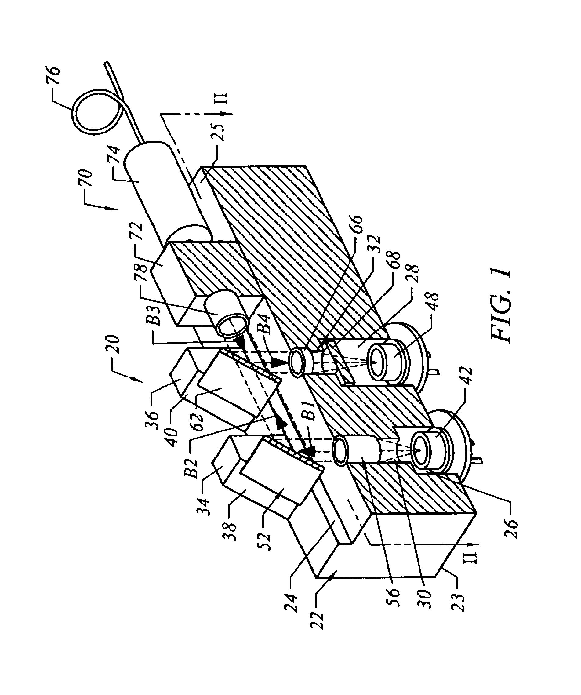
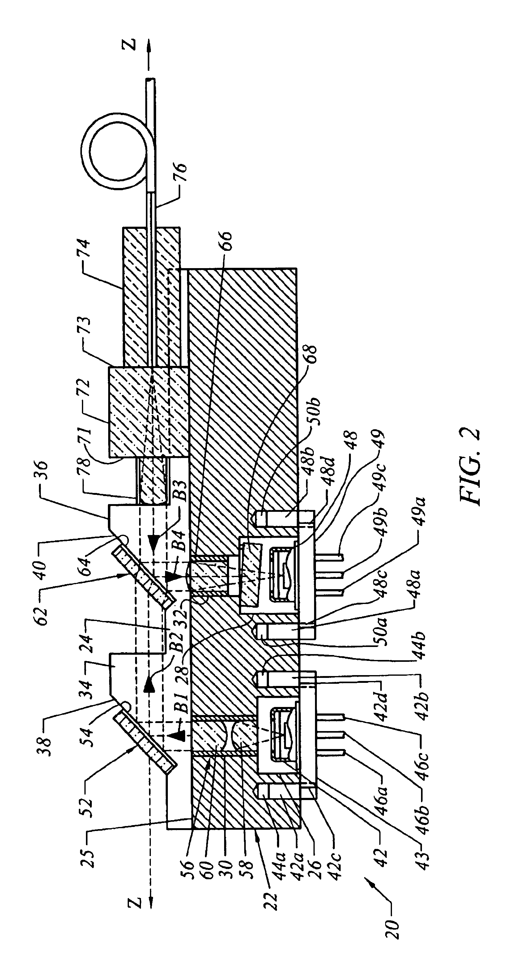
[0030]In an attempt to find a solution for the problems of the prior art, the applicants understood that the problem associated with limitations in transmission speed cased by inductance of the lead wires can be solved by reducing the length of the wires. First the applicants tried to improve the classical orthogonal architecture of a bidirectional transceiver by coupling it with a vertical flexible PC board, then bending the diodes' terminals at 90°, and connecting them to the main PC board. Although this method allowed some increase in the transmission frequency, it appeared to be time and money consuming and not suitable for mass production.

[0031]The applicants also tried to place a laser diode and a photodiode on the same side of the bidirectional transceiver. This allowed direct plugging of the transceiver to holes of the PC board with minimum stray inductance between the laser diode and a laser driver, while electrical assembly of the transceiver on the PCB could be done under...


PUM


Abstract

The optical module of the invention for high-speed bidirectional transceiver consists of a signal receiving unit, a signal transmitting unit, a common receiving-transmitting optical fiber, and a fiber coupling unit. The laser diode and the photodiode are arranged parallel to each other in closely located recesses of the module housing. Such an arrangement makes it possible to shorten distances for guiding lead wires from the terminals of the PC board to the respective terminals of the transmitting and receiving diodes. The laser diode emits a first transmitting laser beam that passes through a microobjective that collimates the beam and directs into onto a full-reflection mirror located inside the module housing. The full-reflection mirror reflects the first transmitting beam at an angle of 90° and transmits it to the end face of an optical fiber through an optical fiber collimator that centers the beam with the fiber core. The module is provided with a second mirror, which is fully transparent to the aforementioned first transmitting beam, but is fully reflective to a second transmitting beam that may propagate in a direction opposite to the first transmitting beam on a different wavelength. Alignment of the optical components is facilitated due to the fact that it is carried out with diffractionally limited and collimated beams.

Description

FIELD OF THE INVENTION[0001]The present invention relates to the field of telecommunication, in particular to bidirectional wavelength division multiplex transmitter / receiver (hereinafter referred to as transceiver) module for use with a single-mode optical fiber in combination with high-speed control electronics. More specifically, the invention relates to a transceiver module having a special architecture that allows for decrease in overall dimensions of the module and for improvement in compatibility with respect to PCBs of high-speed controllers.BACKGROUND OF THE INVENTION[0002]In optical communication systems, the need may arise to multiplex different wavelength signals onto a single fiber. For example, wavelength multiplexing is one method for achieving full bidirectional transmission on a single fiber. In its simplest form, a bidirectional system may comprise two stations, S1 and S2, which transmit information at wavelengths λ1 and λ2, respectively. Thus, station S1 needs a t...

Claims


Application Information

Patent Timeline
IPC IPC(8): G02B6/42
CPCG02B6/4206G02B6/4246G02B6/4214
Inventor GUREVICH, IGORFAIBISHENKO, VICTORFEDYAKIN, NIKOLAIKAKU, SHINKYOVELIKOV, LEONID
Owner MICROALIGN TECH
Learn More