Method for fabricating trench isolations with high aspect ratio

a technology of aspect ratio and trench isolation, which is applied in the manufacture of cable/conductor, basic electric elements, electric apparatus, etc., can solve the problems of incomplete trenches, affecting the isolation between elements, and reducing yield, so as to improve the gap-filling properties of the dielectric layer, improve the effect of thermal annealing speed, and improve the effect of dielectric layer gap-filling properties

Inactive Publication Date: 2005-09-20
NAN YA TECH
View PDF7 Cites 32 Cited by
  • Summary
  • Abstract
  • Description
  • Claims
  • Application Information

AI Technical Summary

Benefits of technology

[0010]In order to overcome the disadvantages of the conventional method, an object of the invention is to provide a method for fabricating trench isolations that improves the gap-filling properties of the dielectric layer and provide a rapid thermal annealing procedure. The invention provides a simple and low-cost fabrication process.
[0012]The present invention combines both LPCVD and HDPCVD with adequate process sequence and conditions. The advantages of this combination are described in the following. The invention eliminates the complicated and expensive multiple deposition and etching cycles required by conventional HDPCVD, thus simplifying the process and reducing the cost thereof. A second dielectric layer with superior dielectric characteristics is deposited on the first dielectric layer, so that the lengthy conventional annealing can be replaced by a rapid thermal annealing procedure, thus improving the characteristics of the second dielectric layer. The anisotropic etching and wet etching using hydrogen fluoride lower the surface of the first dielectric layer, by a specific height, to the opening of the trench, thus filling voids near the opening of the trench and providing improved gap-filling properties.

Problems solved by technology

The conventional high density plasma chemical vapor deposition (HDPCVD) method for fabricating trench isolations with high aspect ratio, in excess of 6, for example, requires multiple deposition and etching cycles, thus it is expensive and offers reduced yield.
Additionally, as the density of integrated circuits increases and element size is reduced, HPCVD provides inadequate step coverage resulting in incompletely filled trenches, and is detrimental to isolation between elements.
Larger voids result in structural instability and reduced element reliability.
Additionally, to improve the inferior TEOS dielectric characteristics it is necessary to perform a high temperature thermal annealing procedure with longer reaction time.
The intensive thermal annealing procedure, however, often adversely affects the peripheral elements.

Method used


Image

  • Method for fabricating trench isolations with high aspect ratio
  • Method for fabricating trench isolations with high aspect ratio
  • Method for fabricating trench isolations with high aspect ratio

Examples


Embodiment Construction

[0019]FIGS. 2A˜2E illustrate cross sections of the method for fabricating a trench isolation according to the invention.

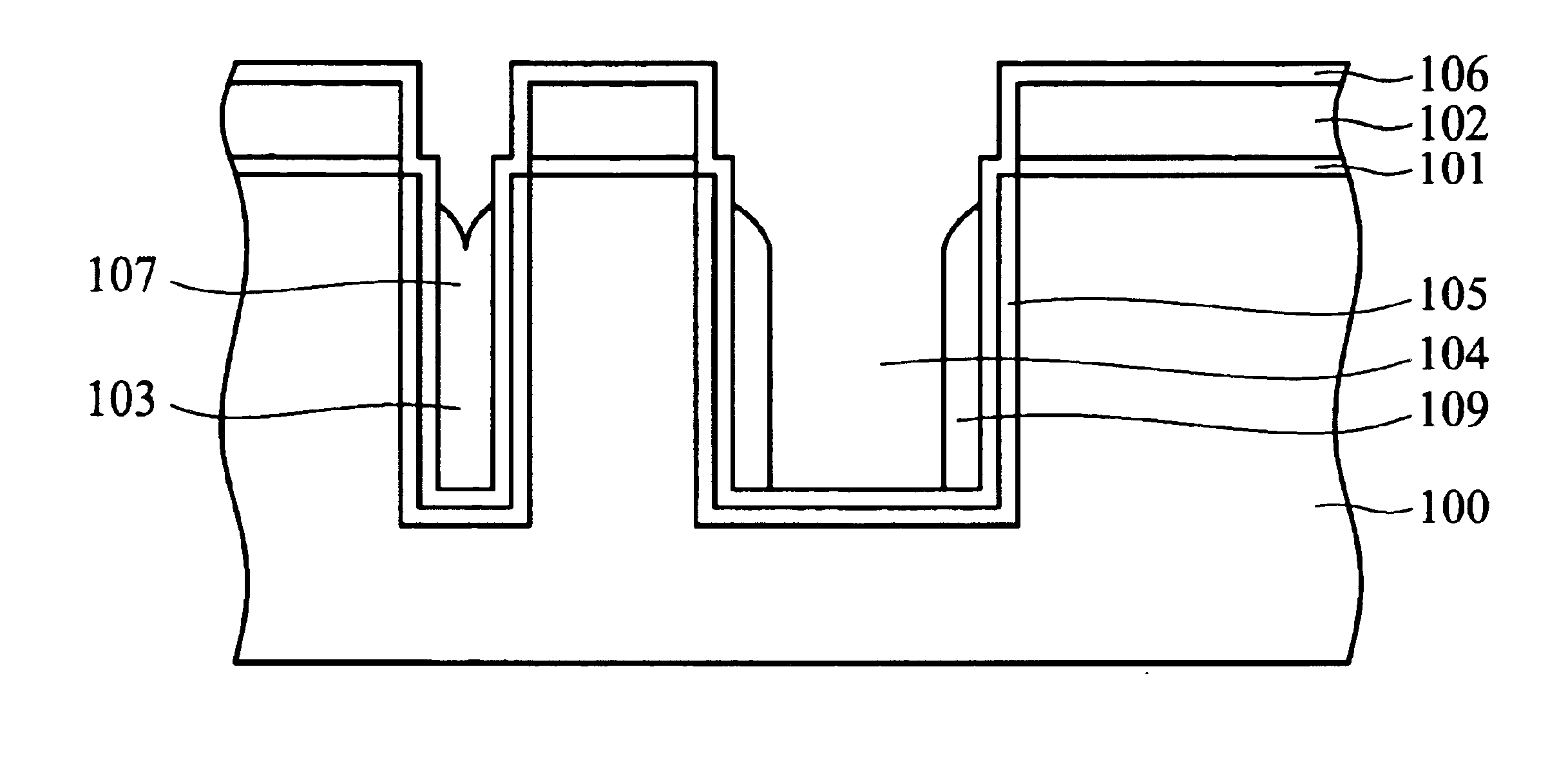
[0020]FIG. 2A, illustrates the initial step of the invention, in which a pad oxide layer 101 is formed on a semiconductor substrate 100, such as a silicon substrate, by CVD or thermal oxidation. A pad nitride layer 102 is then deposited on the pad oxide layer 101 by CVD. The pad oxide layer 101 and the pad nitride layer 102 comprise a pad layer. Next, the pad oxide layer 101 and the pad nitride layer 102 are patterned by photolithography and etching to expose the area of semiconductor substrate 100, where the element isolation region is to be formed. The patterned pad layer is subsequently used as a mask to etch the semiconductor substrate 100; a first trench 103 with a relatively high aspect ratio and a second trench 104 with a relatively low aspect ratio are then formed. Thermal oxidation is performed to grow an oxide liner 105 covering the bottom and sidewalls o...


PUM

PropertyMeasurementUnit
aspect ratioaaaaaaaaaa

Abstract

A method of fabricating a trench isolation with high aspect ratio. The method comprises the steps of: providing a substrate with a trench; depositing a first isolation layer filling the trench by low pressure chemical vapor deposition; etching the first isolation layer so that its surface is lowered to the opening of the trench; depositing a second isolation layer to fill the trench without voids by high density plasma chemical vapor deposition and achieving global planarization by chemical-mechanical polishing then providing a rapidly annealing procedure. Accordingly, the present invention achieves void-free trench isolation with high aspect ratio.

Description

BACKGROUND OF THE INVENTION[0001]1. Field of the Invention[0002]The present invention relates to a method for fabricating semiconductor integrated circuits, and more specifically to a method for fabricating trench isolations with high aspect ratio.[0003]2. Description of the Related Art[0004]Recently, as fabrication techniques for semiconductor integrated circuits have developed, the number of elements in a chip has increased. Element size has integration density has increased. Fabrication line width has decreased from sub-micron to quarter-micron, and smaller. Regardless of the reduction in element size, however, adequate insulation or isolation must be is required among individual elements in a chip so that optimal performance can be achieved. This technique is called device isolation technology. The main object is to form isolations among individual elements, reducing their size as much as possible, ensuring superior isolation while creating more chip space for more elements.[000...

Claims


Application Information

Patent Timeline
Patent Type & Authority Patents(United States)
IPC IPC(8): H01L21/70H01L21/762H01L21/02H01L21/3105H01L21/316H01L21/311
CPCH01L21/76232H01L21/31053H01L21/31116H01L21/31612H01L21/02274H01L21/02164H01L21/02216H01L21/76224
Inventor YANG, SHENG-WEISHIH, NENG-TAILIAO, WEN-SHENGCHANG, CHIH-HOW
Owner NAN YA TECH
Why Eureka
Try Eureka