

Catoptric projection optical system, exposure apparatus and device fabrication method using same
a catoptric and optical system technology, applied in the field of exposure apparatuses, can solve the problems of difficult to meet the requirements of using, the optical system could not include any lenses, and the high na is difficult to maintain, and achieves the effects of small maximum effective diameter, good imaging performance, and small span
- Summary
- Abstract
- Description
- Claims
- Application Information
AI Technical Summary
Benefits of technology
Problems solved by technology
Method used
Image

Examples
Embodiment Construction
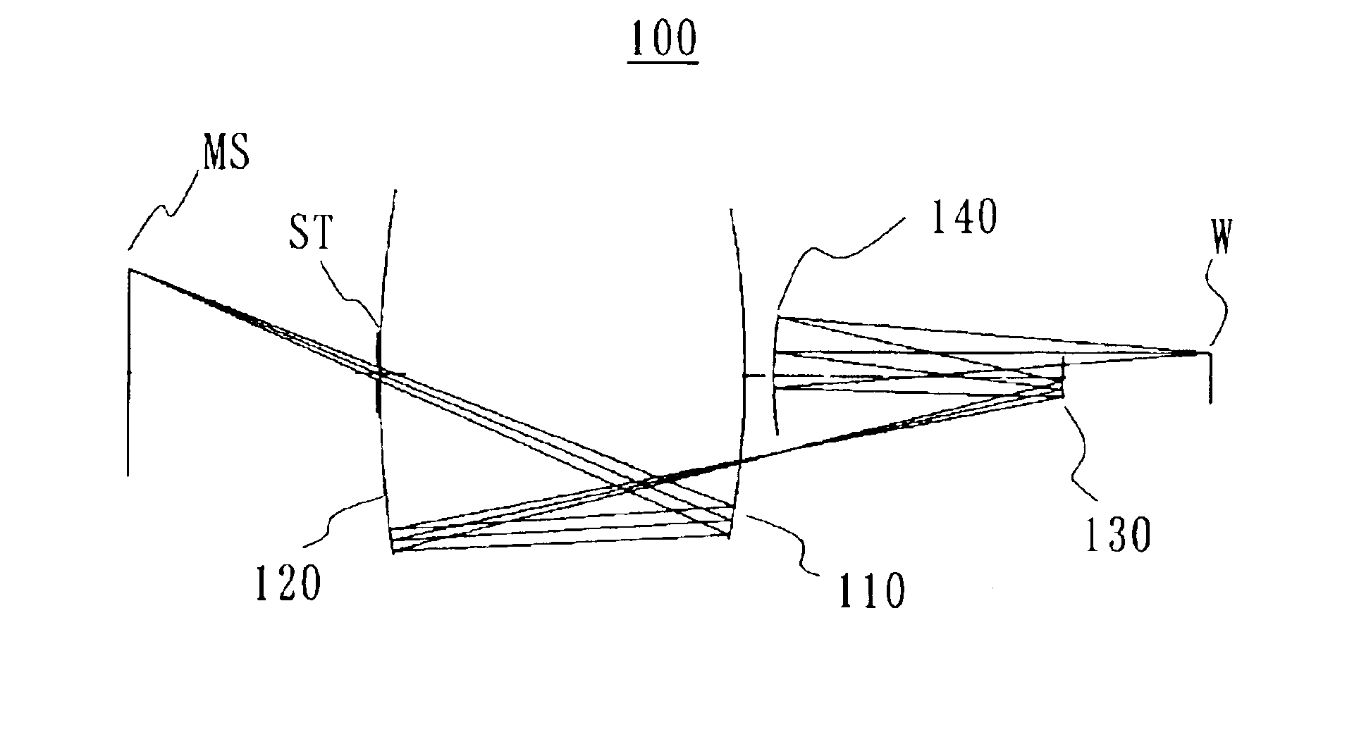
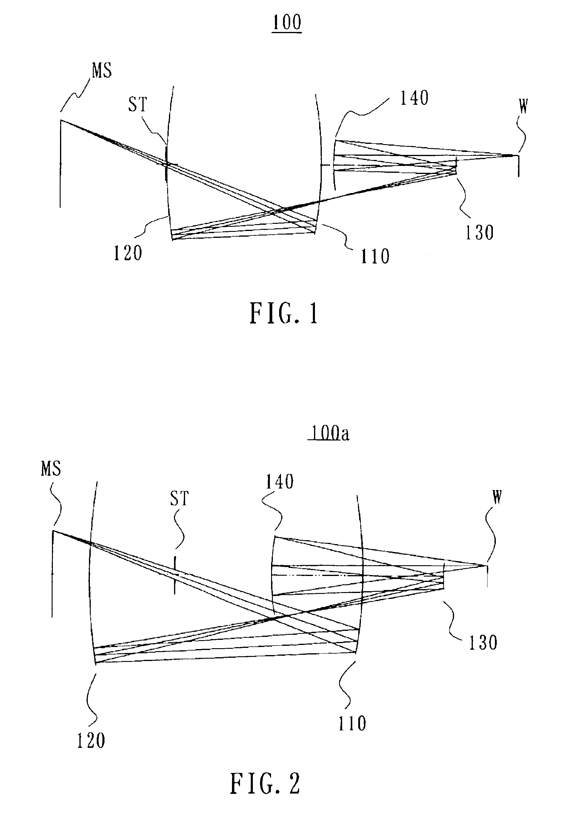
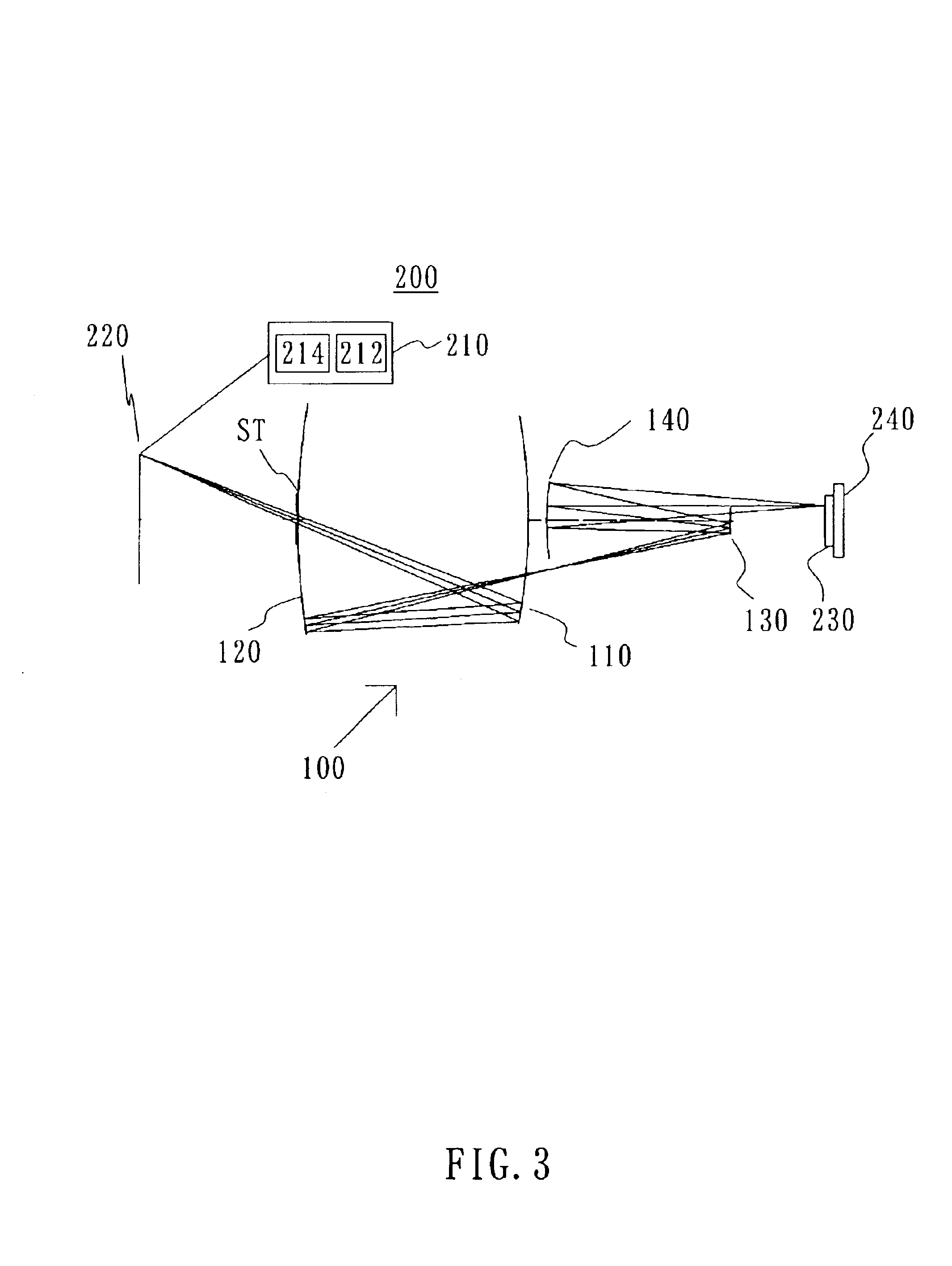
[0022]A description will now be given of catoptric projection optical system 100 and an exposure apparatus 200 as one aspect of the present invention with reference to the accompanying drawings. The present invention is not limited to these embodiments and each element is replaceable within a scope that achieves the objects of the present invention. The same reference numeral in each figure denotes the same element, and a description thereof will be omitted. Here, FIG. 1 is a schematic sectional view showing the catoptric projection optical system 100 and its optical path of one embodiment according to the present invention. FIG. 2 is a schematic sectional view showing a catoptric projection optical system 100a and its path as a variation of the catoptric reduction projection optical system 100 shown in FIG. 1. Unless otherwise specified, the catoptric projection optical system 100 generalizes the catoptric reduction projection optical system 100a.
[0023]Referring to FIG. 1, the inv...
PUM
| Property | Measurement | Unit |
|---|---|---|
| size | aaaaa | aaaaa |
| size | aaaaa | aaaaa |
| wavelength | aaaaa | aaaaa |
Abstract
Description
Claims
Application Information