Radiant heating source with reflective cavity spanning at least two heating elements

a technology of radial heating source and reflective cavity, which is applied in the field of heating source, can solve the problems of overexposure to plasma, subsequent damage of wafers, and limited time and surface uniformity of heating and gas delivery components of wafer processing systems,

Inactive Publication Date: 2005-09-20
AXCELIS TECHNOLOGIES
View PDF20 Cites 16 Cited by
  • Summary
  • Abstract
  • Description
  • Claims
  • Application Information

AI Technical Summary

Benefits of technology

[0020]The present invention provides a radiant heating device with high consistency of heating conditions in both a radial and an azimuth orientation across a plane of a workpiece such as a wafer. Use of a reflective inner wall and angled radiant energy bulbs combined with an optimized shape of the inner and outer wall and bottom reflecting surfaces (in one embodiment the radiant heating device is oriented to have what can be referred to as a bottom surface) provide uniform heat distribution over a wafer surface with a more compact design. A radiant heater constructed in accordance with one embodiment of the invention results in more uniform processing parameters across the wafer surface as well as more uniform process speed and heating effectiveness.
[0021]The reflector structure of one embodiment of the invention involves plane surfaces and / or simple surfaces of revolution shaped to provide a better uniformity of process conditions and highly effective energy use.
[0022]The relatively flat non-focusing planar, cone, cylindrical or convex curved reflecting surfaces reflect heat energy from a group of or all of the heating elements and do not focus an individual bulb's energy at the workpiece region. A convex (as seen from a position of the heating elements) internal wall disperses energy of each bulb to the even wider area of wafer surface and makes heat delivered to the wafer from each bulb smoother, less concentrated. The effect is opposite to the focusing property of prior art parabolic or elliptical or similar, concave (as seen from a position of the elements) surfaces, including a cylinder outer wall type design. Energy from each individual bulb reflected from a prior art concave surface is concentrated at a smaller area of the wafer and equalizing participation of other bulbs at this concentrated area is less. Practice of the invention lessens non-uniformity caused by prior art heating devices caused by individual or group tolerances resulting from manufacturing and assembly because the heating at each locale is a result of an increased superposition of energy from many bulbs that makes deviations of individual properties of each bulb / reflector less pronounced.
[0023]A defocusing effect can be made even stronger if outer wall reflecting surface is made to be convex (as seen from a position of the heating elements). In one embodiment a convex outer wall portion formed from a curved line rotated about a center axis is used. This effect could also be used on a bottom and on inner surfaces of revolution, adding (as seen from the position of the bulbs) more convexity in direction perpendicular to the natural convexity of the inner cylinder or cone. This produces additional defocusing or divergence of radiative heat reflected on the bottom and outer wall reflecting surfaces.
[0029]It is still a further object of invention to provide heating elements spatial positioning independent from their electrical connection attachment for more consistent filament alignment in relation to the heating target surface.

Problems solved by technology

Unfortunately, the heating and process gas delivery are under control of separate process tool components and depend on the geometry and construction of the processing unit.
Prior art heating and gas delivery components of a wafer processing system have been limited in achieving time and surface uniformity of action.
The process non-uniformity can result in overexposure to plasma with the subsequent damage of the wafers and other negative effects.
During stripping, the non-uniformity slows the resist cleaning speed and therefore causes a decrease of wafer throughput of the stripping process.
If the heater design cannot compensate enough or overcompensates, a radial process non-uniformity results.
This component of non-uniformity is mostly a result of a local asymmetry that is specific to the process chamber / gas supply system design or is produced by different tolerances in the system.
Simultaneous achievement of both thermal uniformity and uniform active ingredient concentration to the region of the wafer over the process area can be difficult to provide.
For example, process gas supply and process gas exhaust design for downstream microwave ashers can cause substantial radial and azimuth non-uniformity in active species delivery.
The system disclosed in the '555 patent also exhibits certain problems.
This prior art arrangement can result in azimuthal and especially radial non-uniformity of the temperature and, therefore, processes speed non-uniformity.
An additional source of non-uniformity is inconsistency of an individual reflector's shape, finish quality, position and orientation due to dimensional tolerances of the reflector's and bulb mountings.
The numerous manufacturing and assembly tolerances also include individual bulb intensity, filament spatial position, reflectors and bulbs base installation that can result in non-uniformity of temperature and therefore, processing rate.
The minimization of all individual bulb positioning tolerances, extending from the wafer surface through the heating chamber and heater design, to the filament spatial orientation appears to be difficult to achieve.
The random combination of tolerances for newly built heaters in some cases has caused high non-uniformity and required the whole assembly to be rejected during manufacture.
An individual parts alignment and selection in this cases is not sufficient.
In addition, power zoning during the wafer temperature ramp up is evidence of inefficient power usage for heating.
This is a natural problem of any pan-shaped one-wall asymmetric design where the radiant energy directed to the center axis is not under designer control i.e. energy is not redirected to the proper area of the wafer to improve uniformity.
Another problem with tubular or pan-shaped reflectors is loss of part of the bulb energy which is directed parallel or close to parallel to the wafer plane.
The total heating effectiveness of a such an array drops due to the absorbed energy lost without heating the wafer.
Analysis of the equipment built in conformity with the '072 patent shows that the principal effect of the part-to-part deviation is azimuth temperature non-uniformity.
Note, that for each individual bulb there is an effect of non-uniformity amplification because of the focusing effect of each individual bulb in a direction across the parabolic areas of the reflector surface.

Method used


Image

  • Radiant heating source with reflective cavity spanning at least two heating elements
  • Radiant heating source with reflective cavity spanning at least two heating elements
  • Radiant heating source with reflective cavity spanning at least two heating elements

Examples


Embodiment Construction

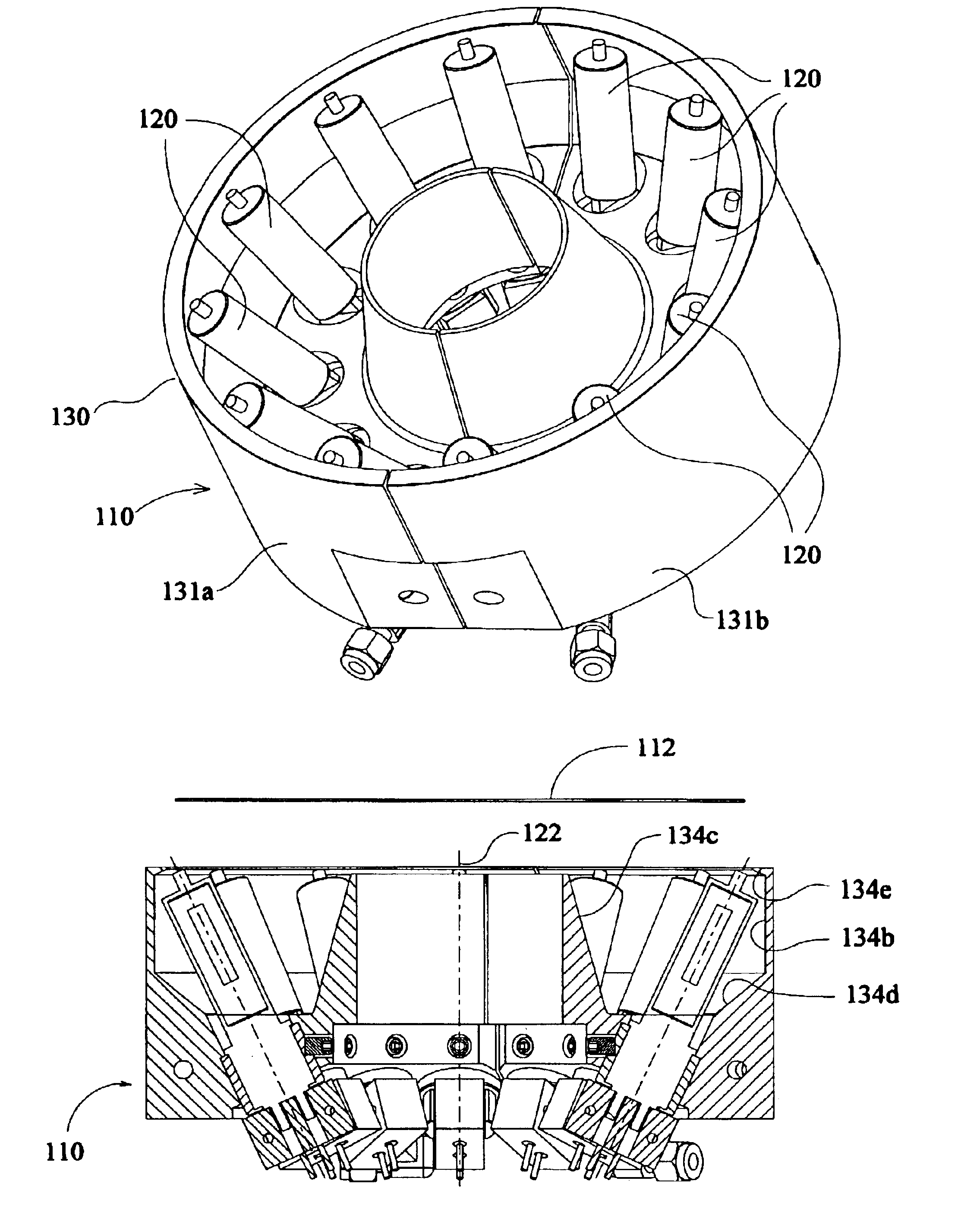
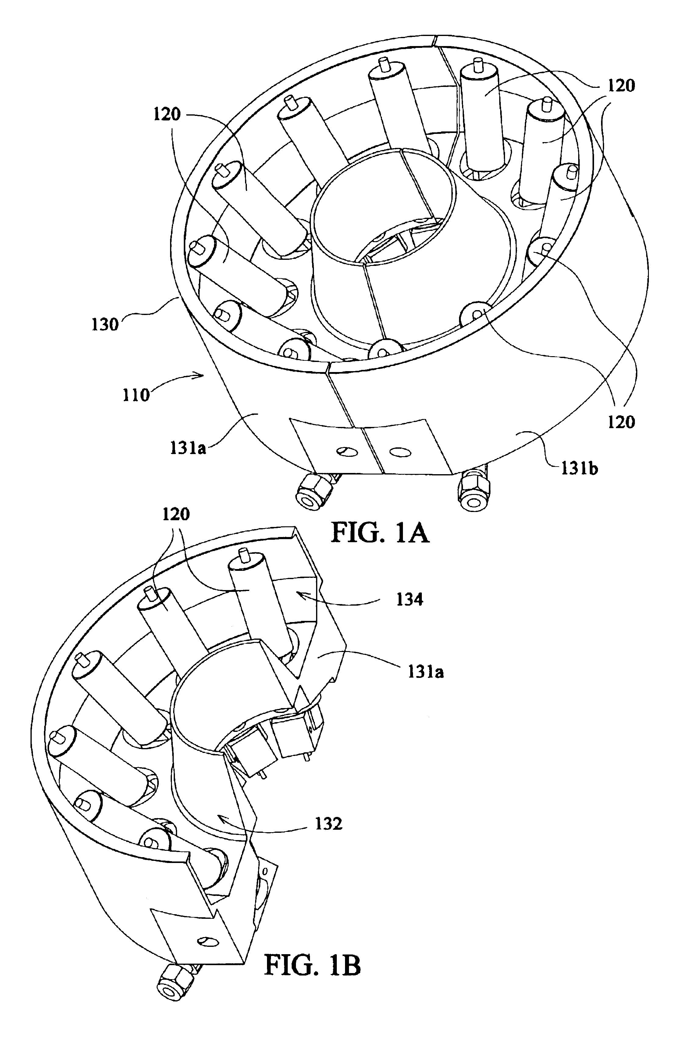
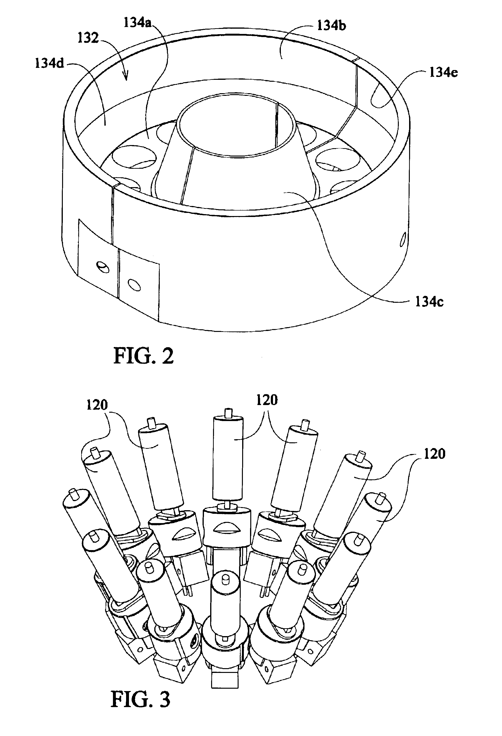
[0051]FIG. 19 is a plan view of a prior art radiant lamp array for wafer heating in semiconductor processing chambers. FIG. 20 shows a perspective view of the apparatus of FIG 19. These depictions are similar to depictions shown in U.S. Pat. No. 6,023,555 to Penelon et al. The '555 patent is incorporated herein by reference. In each depiction, one half of an array of heating elements of sources is shown, the second half which is not shown is symmetric to the part shown in FIGS. 19 and 20. In the plan view of the FIG. 19 are also shown four of the eight individual heating elements 1. As described in the '555 patent they are quartz halogen bulbs.

[0052]FIGS. 19 and 20 also depict ellipsoidal shaped back reflectors 2 combined with the adjacent tubular reflectors 3 which have reflector surfaces that extend in a direction parallel to an elongated axis of an associated heating lamp. Each of the ellipsoidal and tubular reflectors is mounted next to an associated a single bulb heating elemen...


PUM


Abstract

A radiant source for heating a workpiece such as a semiconductor wafer includes a plurality of radiant heating elements, arranged in an array that is generally concentric about a source center axis. A reflector has a reflecting surface that bounds a cavity or channel that contains the heating elements, the reflector comprising walls that extend around the center axis and that are finished for reflecting radiant energy emitted by the heating elements to a region occupied by a wafer. The channel reflecting surfaces comprise at least a part of a plane and / or cylinder and / or a cone and / or a convex to the heating elements curved surface of revolution bordering or spanning two or more adjacent heating elements.

Description

FIELD OF INVENTION[0001]The invention relates to a heating source and more particularly to a heating source used in heating a workpiece such as a semiconductor wafer or similar object and more particularly to temperature dependent processes where the workpiece is heated with a heat radiating source.BACKGROUND OF THE INVENTION[0002]The speed of several types of semiconductor wafer processing depends on a process gas active ingredient concentration or delivery rate at the region of the wafer surface and also on the substrate temperature maintained at the wafer surface. A goal of treatment systems is to provide uniform temperature and active ingredients distributions across the wafer process area. In certain circumstances it is also important to maintain control over these process parameters during a temperature ramping period of a treatment process.[0003]Unfortunately, the heating and process gas delivery are under control of separate process tool components and depend on the geometry...

Claims


Application Information

Patent Timeline
Patent Type & Authority Patents(United States)
IPC IPC(8): H01L21/00
CPCH01L21/67115H01L21/324H01L21/02
Inventor GARMER, CHRISTOPHER J.KLEYNER, FELIKS B.AYZMAN, ILYA M.GOLDMAN, IGOR L.
Owner AXCELIS TECHNOLOGIES
Why Eureka
Try Eureka