Semiconductor memory device and method for manufacturing the same

a memory device and semiconductor technology, applied in semiconductor devices, electrical devices, capacitors, etc., can solve the problems of inability to perform metal interconnection processes well, the area per cell also decreases so as to improve the electrical characteristics of the memory device, the contact area is increased greatly, and the contact resistance is substantially reduced

Inactive Publication Date: 2005-09-27
SAMSUNG ELECTRONICS CO LTD
View PDF1 Cites 9 Cited by
  • Summary
  • Abstract
  • Description
  • Claims
  • Application Information

AI Technical Summary

Benefits of technology

[0024]In the semiconductor memory device and the method for manufacturing the same as disclosed herein, the guard-ring pattern is formed in a boundary between the cell area and the peripheral circuit area while surrounding the cell area, and thereby a step caused by manufacturing the stack-shaped capacitor is removed during a manufacturing process. In addition, the contact fill for the plate elec

Problems solved by technology

However, as the memory device becomes highly integrated, its design rule becomes extremely dense and an area for each memory device becomes narrower, and thus, area per cell also decreases.
However, in the stack-shaped capacitor, when the stack-shaped capacitor forms a storage node, a step between the cell area and a peripheral area becomes very severe.
As a result, a metal interconnection process cannot be performed well due to an extreme pattern-thinning phenomenon caused

Method used


Image

  • Semiconductor memory device and method for manufacturing the same
  • Semiconductor memory device and method for manufacturing the same
  • Semiconductor memory device and method for manufacturing the same

Examples


Embodiment Construction

[0030]The present invention will be described more fully hereinafter with reference to the accompanying drawings in which preferred embodiments of the invention are shown. This invention may, however, be embodied in many different forms and should not be construed as being limited to the embodiments set forth herein. Rather, these embodiments are provided so that this disclosure will be thorough and complete, and will fully convey the scope of the invention to those skilled in the art. In the drawings, the forms of elements are exaggerated for clarity.

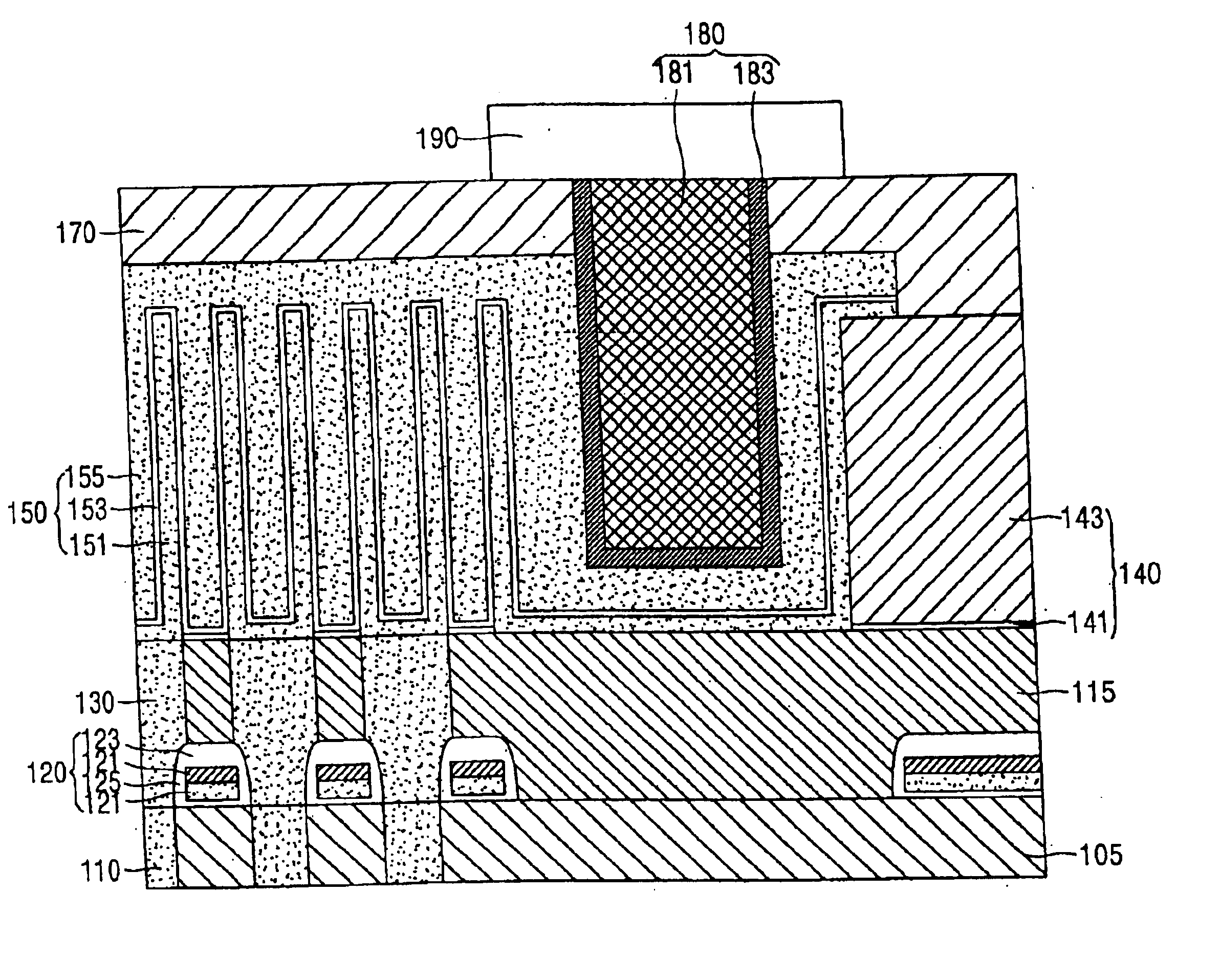
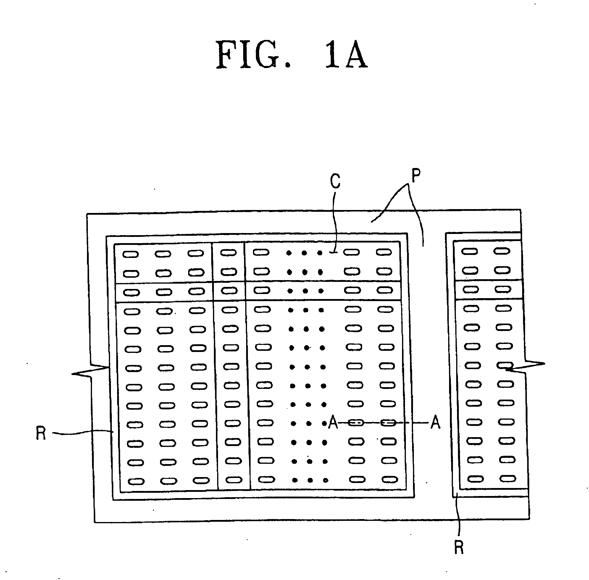
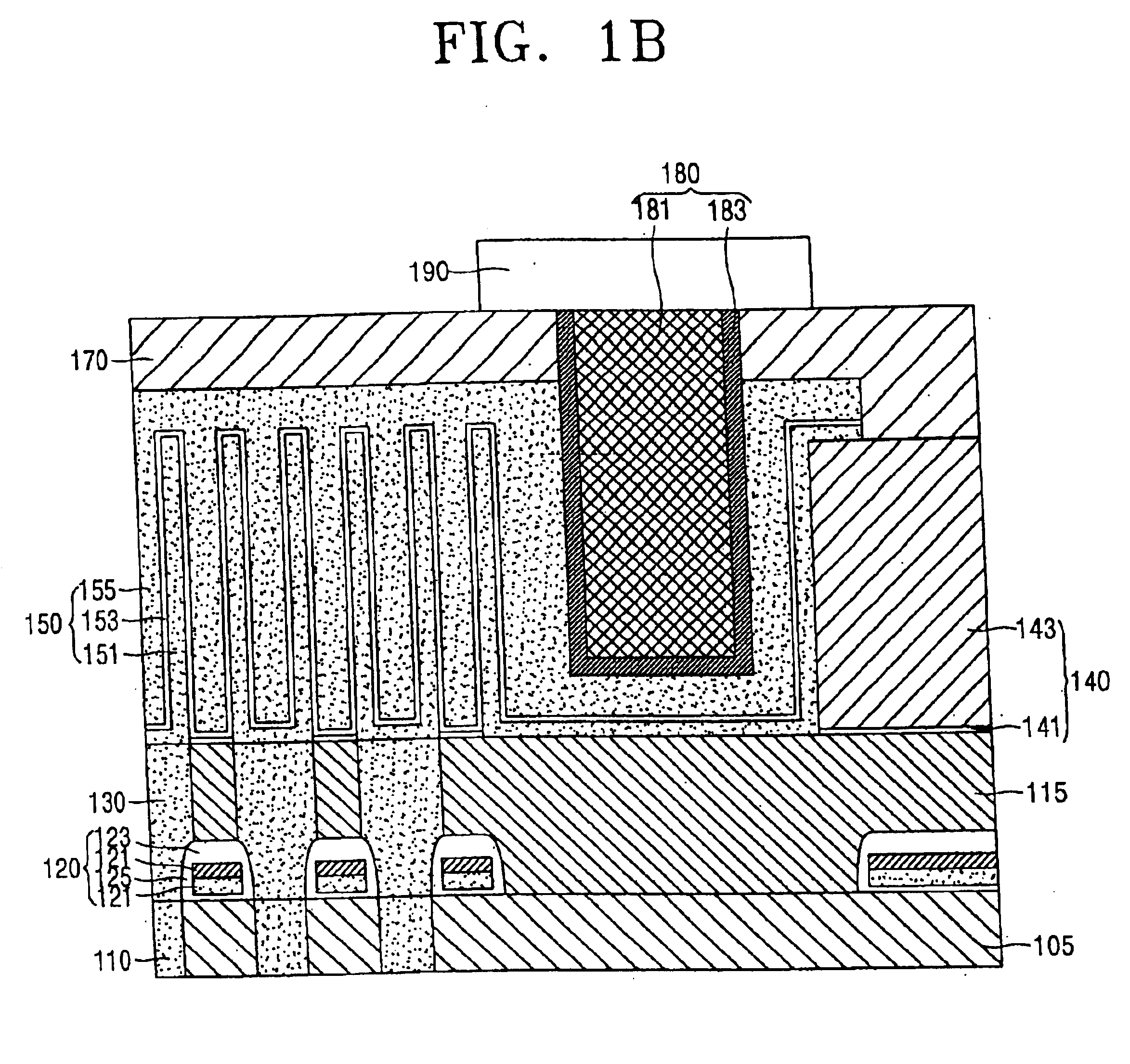
[0031]FIG. 1A is a plane view of a semiconductor memory device according to an embodiment of the present invention, and FIG. 1B is a cross-sectional view taken along line A—A of FIG. 1A.

[0032]Referring to FIGS. 1A and 1B, the semiconductor memory device includes a cell area C in which memory devices are formed in a matrix shape, and a peripheral circuit area P formed to exchange signals with the memory devices. Included in the cell are...


PUM


Abstract

A semiconductor memory device and a method for manufacturing the same are provided. The semiconductor memory device includes an oxide layer for isolating individual devices which define device areas so that a cell area and a peripheral circuit area are separated from each other on a semiconductor substrate, a plurality of MOS transistors, which are comprised of source areas, drain areas, and gates that are formed in the cell area and the peripheral circuit area, a bit line, which is formed on the plurality of MOS transistors and is electrically connected to the MOS transistor, a stack-shaped capacitor, which is comprised of a first electrode, a dielectric layer, and a second electrode between which the MOS transistors and the bit line in the cell area is interposed, a guard-ring pattern, which are interposed between the cell area and the peripheral circuit area, surrounds the cell area and is apart from the peripheral circuit area, and a contact fill for plate electrode, which is formed in the guard-ring pattern and is in contact with the second electrode that is formed on the internal sidewall and the bottom of the guard-ring pattern. The guard-ring pattern is formed in a boundary between the cell area and the peripheral circuit area while surrounding the cell area, and thereby step caused by manufacture of the stack-shaped capacitor are removed during a manufacturing process, and the contact fill for plate electrode is formed in the guard-ring pattern, and thereby the ground resistance of the capacitor is reduced, and the electrical characteristics of the memory device are improved.

Description

CROSS REFERENCES TO RELATED APPLICATIONS[0001]This application is a divisional of U.S. patent application Ser. No. 10 / 246,392 filed on 19 Sep. 2002 now U.S. Pat. No. 6,727,542, and claims priority under 35 U.S.C. §119 from Korean Patent Application No. 2002-2509, filed on 16 Jan. 2002, the entirety of each of which is hereby incorporated by reference as if fully set forth herein.BACKGROUND[0002]1. Field of the Invention[0003]The present invention relates to a semiconductor memory device and method for manufacturing the same, and more particularly, to a dynamic random access memory (DRAM) having a stack-shaped capacitor and a method for manufacturing the same.[0004]2. Description of the Related Art[0005]A dynamic random access memory (DRAM) among semiconductor memory devices is comprised of one transistor and one capacitor. Thus, in order to serve as a memory device, the DRAM must have sufficient capacitance. There is no problem when the design rule of the memory device is wide. Howe...

Claims


Application Information

Patent Timeline
IPC IPC(8): H01L21/70H01L21/02H01L21/60H01L21/8242H01L27/108
CPCH01L21/76897H01L27/10894H01L28/91H01L27/10814H01L27/10852H01L27/10882H01L28/55H10B12/315H10B12/48H10B12/033H10B12/09H10B12/00
Inventor KIM, KI-NAMPARK, BYUNG-JUN
Owner SAMSUNG ELECTRONICS CO LTD
Why Eureka
Try Eureka