Organic bistable device and organic memory cells

a bistable device and organic technology, applied in solid-state devices, nanoinformatics, instruments, etc., can solve the problems of complex architecture, reduced electroluminescence of doped polymers, and relatively long time-consuming rotation of dipole groups

Inactive Publication Date: 2005-09-27
RGT UNIV OF CALIFORNIA
View PDF10 Cites 113 Cited by
  • Summary
  • Abstract
  • Description
  • Claims
  • Application Information

AI Technical Summary

Benefits of technology

[0012]In accordance with the present invention, bistable electrical devices are provided that are convertible between a low resistance (impedance) state and a high resistance (impedance) state. The bistable electrical devices are well suited for use as electrical switching and memory devices. The bistable electrical devices of the present invention include a bistable body whic...

Problems solved by technology

Unfortunately, rotation of the dipole groups takes a relatively long time.
Also, doping of the polymer reduces the electroluminescence of the doped polymer.
Although these inorganic devices have been technically and commercially successful, they have a number of drawbacks including complex architecture and high fabrication cost...

Method used


Image

  • Organic bistable device and organic memory cells
  • Organic bistable device and organic memory cells
  • Organic bistable device and organic memory cells

Examples


example 1

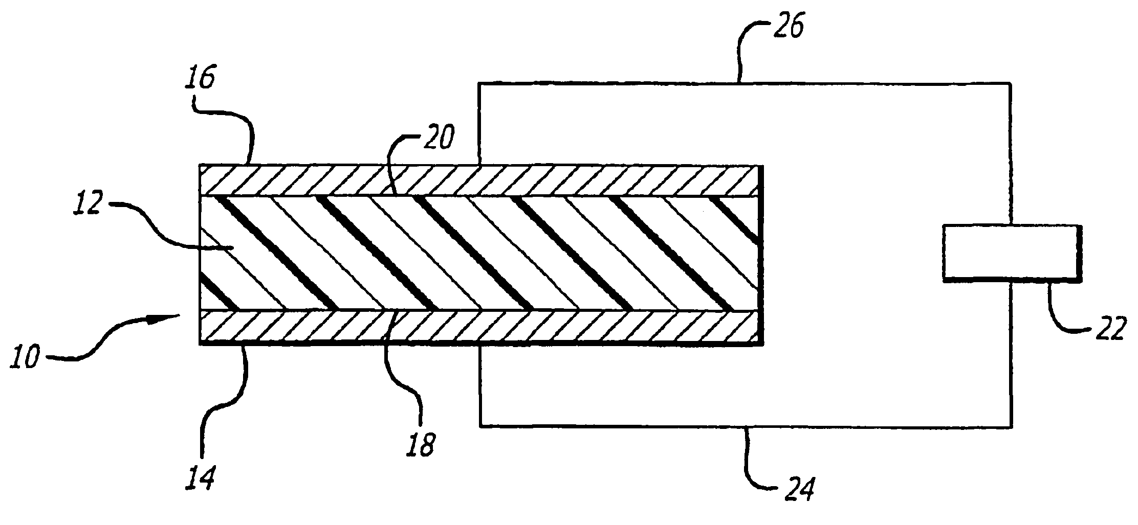
[0049]A bistable device was fabricated as shown in FIG. 2. The first step in the fabrication of the device involved the vacuum deposition of a layer (50 nm thick) of aluminum (Al) on top of a pre-cleaned glass substrate. This Al functioned as the anode layer 36 of the device. Next, the first low conductivity layer 32, the thin metal layer 30, and the second low conductivity layer 34 were sequentially evaporated on top of the Al anode layer 36. Then, the cathode metal (Al) was evaporated onto the top layer 34 to form a cathode layer 42 which was 50 nm thick. The depositions were carried out in a vacuum of about 1×10⁻⁶ torr and the thickness of the depositing species controlled by a quartz crystal monitor. The low conductivity layers 32 and 34 were 40 nm thick with the central high conductivity layer 30 being 20 nm thick. Aluminum was used for the central layer 30. 2-amino-4-5-imidazoledicarbonitrile (AIDCN) was used for the two low conductivity layers (32 and 34).

[0050]The I-V curves...

example 2

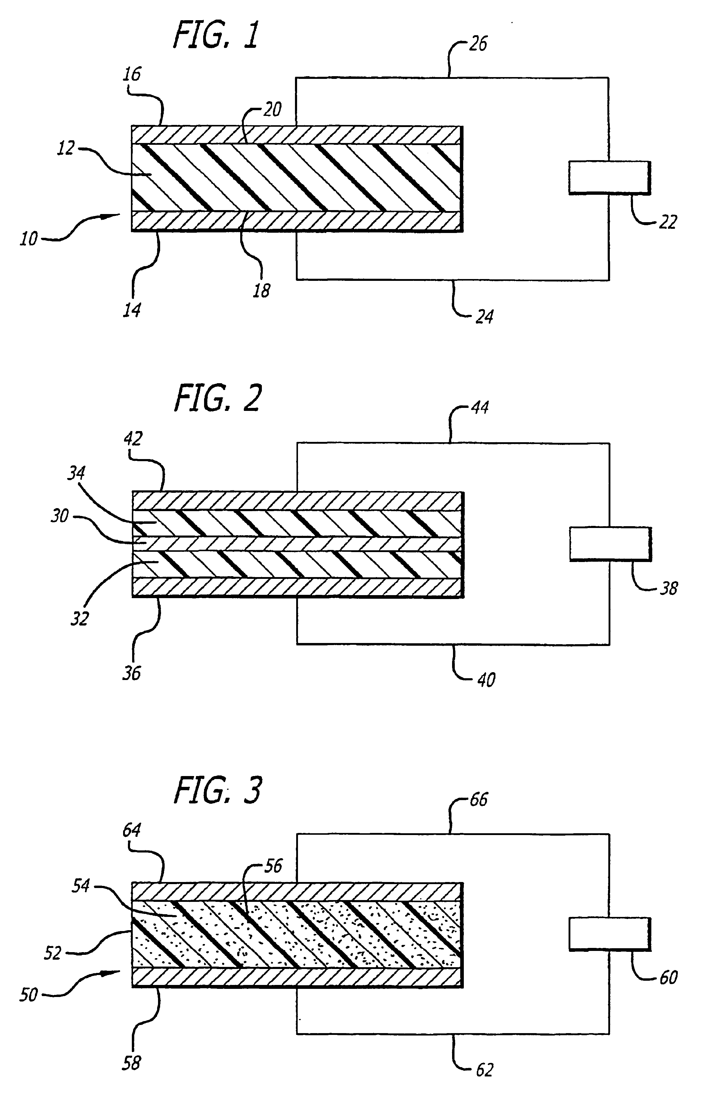
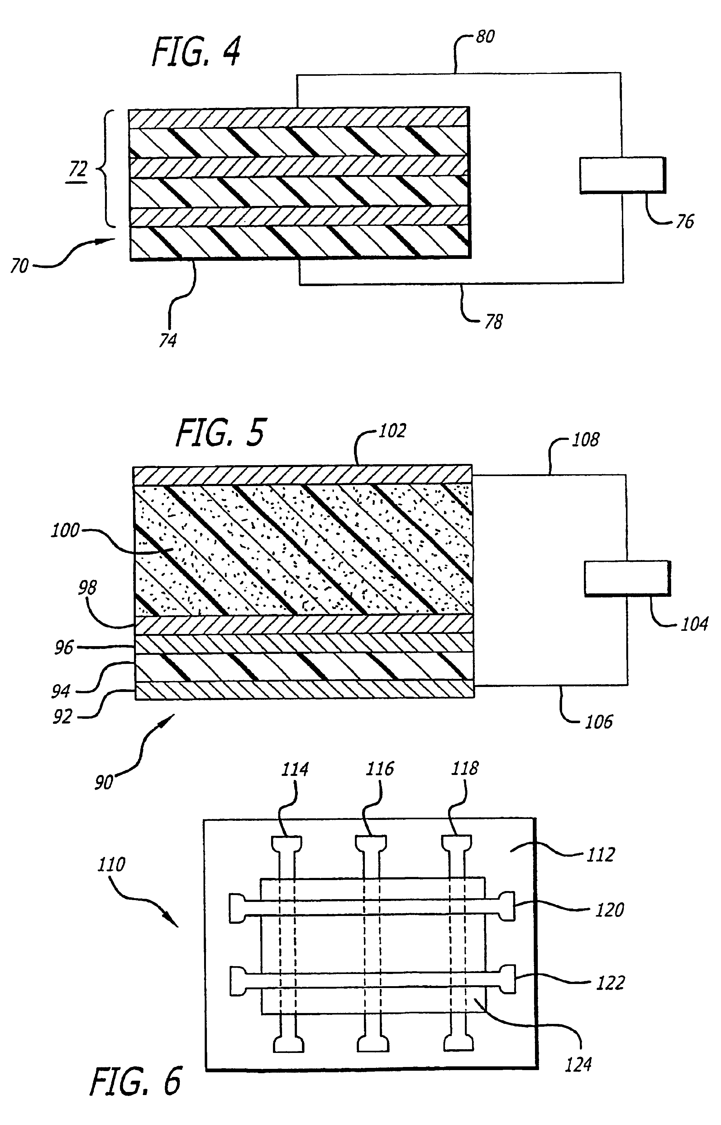
[0051]A bistable device was made in the same manner as Example 1 except that three high conductivity Al layers (each 20 nm thick) were deposited between alternating layers of AIDCN (each 20 nm thick). The device exhibited bistable characteristics in that the conductivity changed from 10−11 to 10−8 (1 / ohm.cm) upon application of a 5 V. bias. The device was convertible back to a low conductivity state by application of a −5V bias.

example 3

[0052]A bistable device was made in the same manner as Example 1 except that Cu was substituted for Al as the high conductivity material in layer 30. The Cu layer was 33 nm thick and the two AIDCN layers 32 and 34 were 50 nm thick. The I-V curves are shown in FIG. 8 where it can be seen that the transition from the high resistance state to low resistance state is accompanied by a sharp change in current up to 5 orders in magnitude. FIG. 9 shows I-V curves for multiple sweeps. The numbers next to the curves correspond to the bias sweep sequence. The multiple sweeps shown in FIG. 9 demonstrate that the transition is reversible.


PUM


Abstract

A bistable electrical device (50) employing a bistable body (52) and a high conductivity material (54). A sufficient amount of high conductivity material (54) is included in the bistable body (52) to impart bistable between a low resistance state and a high resistance state by application of an electrical voltage (60).

Description

RELATED APPLICATION[0001]This application is a 371 of PCT / US01 / 17206, filed May 24, 2001, claims the benefit of U.S. Provisional Application No. 60 / 244,734, filed Oct. 31, 2000.[0002]This invention was made with Government support under Grant No. N00014-98-1-0484, awarded by the Office of Naval Research. The Govemment has certain rights in this invention.BACKGROUND OF THE INVENTION[0003]1. Field of the Invention[0004]The present invention relates generally to electronic memory cells and switches. More particularly, the present invention involves electronic memory devices which utilize memory elements that exhibit bistable electrical behavior.[0005]2. Description of Related Art[0006]The publications and other reference materials referred to herein to describe the background of the invention and to provide additional details regarding its practice are hereby incorporated by reference. For convenience, the reference materials are numerically referenced and identified in the appended bi...

Claims


Application Information

Patent Timeline
IPC IPC(8): G11C16/02G11C13/02G11C13/00G11C11/34G11C11/54H01L27/10H01L27/28H01L45/00H01L49/02H01L51/05H01L51/30
CPCB82Y10/00G11C11/34G11C11/54G11C13/0004G11C13/0014G11C13/0016H01L45/04H01L45/1233H01L45/14H01L27/2409H01L27/2472G11C2213/12G11C2213/15G11C2213/55G11C2213/56H10B63/82H10B63/20H10N70/20H10N70/881H10N70/826
Inventor YANG, YANGMA, LIPINGLIU, JIE
Owner RGT UNIV OF CALIFORNIA
Why Eureka
Try Eureka