Multi-cell organic memory element and methods of operating and fabricating

a memory element and organic technology, applied in the field of multi-cell organic memory devices, can solve the problems of increasing the volume, use and complexity of computers and electronic devices, reducing the efficiency of data storage, so as to facilitate the migration of charge, improve the utilization rate and density, and short resistance/impedance switch time

Inactive Publication Date: 2005-05-31
MONTEREY RES LLC
View PDF1 Cites 11 Cited by
  • Summary
  • Abstract
  • Description
  • Claims
  • Application Information

AI Technical Summary

Benefits of technology

[0010]The present invention relates to systems and methods for fabricating multi-cell organic semiconductor memory devices. Multi-dimension memory structures composed of organic material such as polymer are formed within an Inter Layer Dielectric (ILD) of an organic semiconductor memory device. The structures can be substantially any shape such as cylindrical and are typically formed in a void in the ILD such as through a via or other type relief. The structures are formed over a passive layer which in turn is formed over a conductive material such as copper. After the memory structures are formed over the passive and conductive layers, respectively, one or more conductive electrodes can be placed over various portions of the memory structures to form one or more memory cells within selected portions of the memory structure. In this manner, memory device utilization, density, and packing can be substantially improved. The memory cells are activated b

Problems solved by technology

The volume, use and complexity of computers and electronic devices are continually increasing.
However, silicon-based devices are approaching their fundamental physical size limits.
Inorganic solid-state devices are generally encumbered with a complex architecture which leads to high cost and a loss of data storage density.
The volatile semiconductor memories based on inorganic semiconductor material must constantly be supplied with electric current with a resulting heating and high electric power consumption in order to maintain stored information.
Non-volatile semiconductor devices have a reduced data rate and relatively high power consumption and large degree of complexity.
Moreover, as the size of inorganic solid-state devices decreases and integration increases, sensitivity to alignment tolerances increases making fabrication markedly more difficult.
Scaling inorganic solid-state devices raises issues with dopant diffusion lengths.
As dimensions are reduced, the dopant diffusion lengths in silicon are posing difficulties in process design.
However, it is not clear that such accommodatio

Method used


Image

  • Multi-cell organic memory element and methods of operating and fabricating
  • Multi-cell organic memory element and methods of operating and fabricating
  • Multi-cell organic memory element and methods of operating and fabricating

Examples


Embodiment Construction

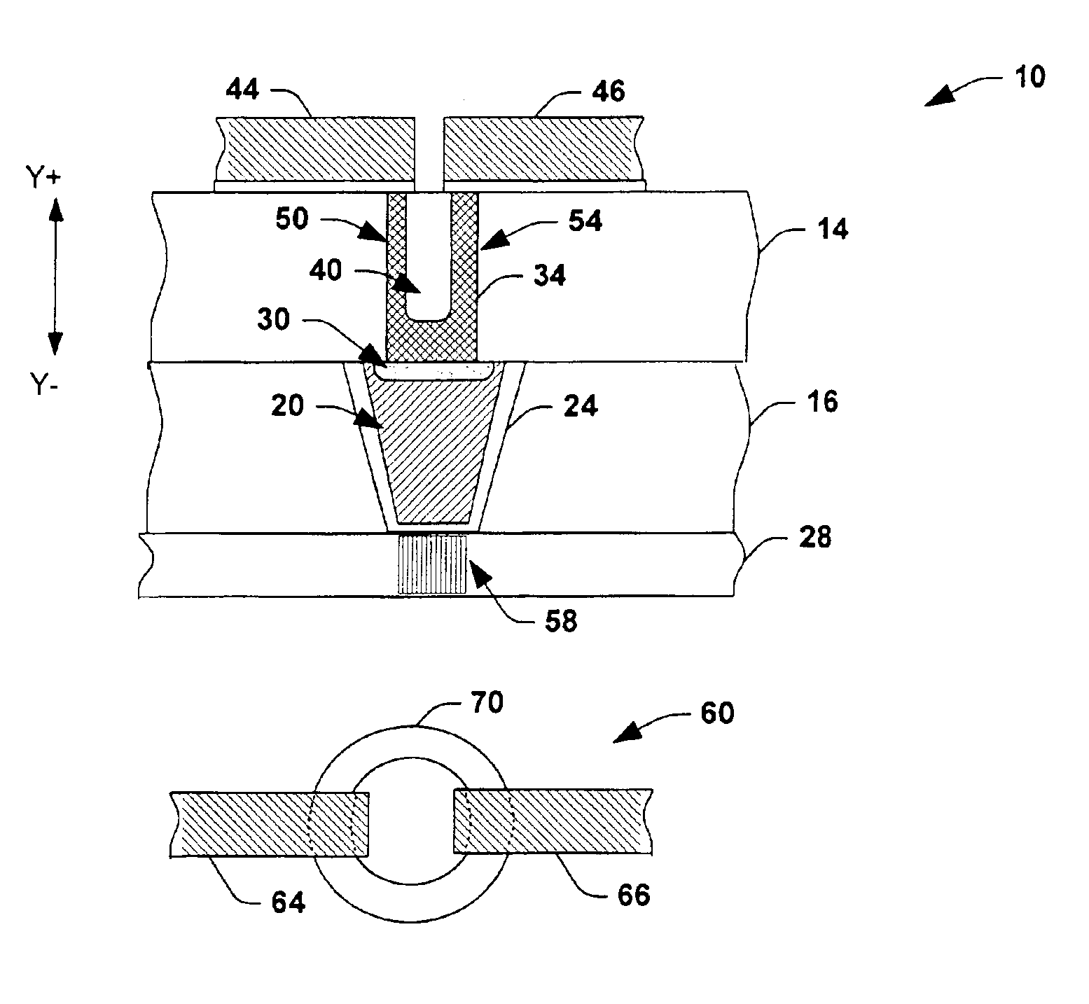
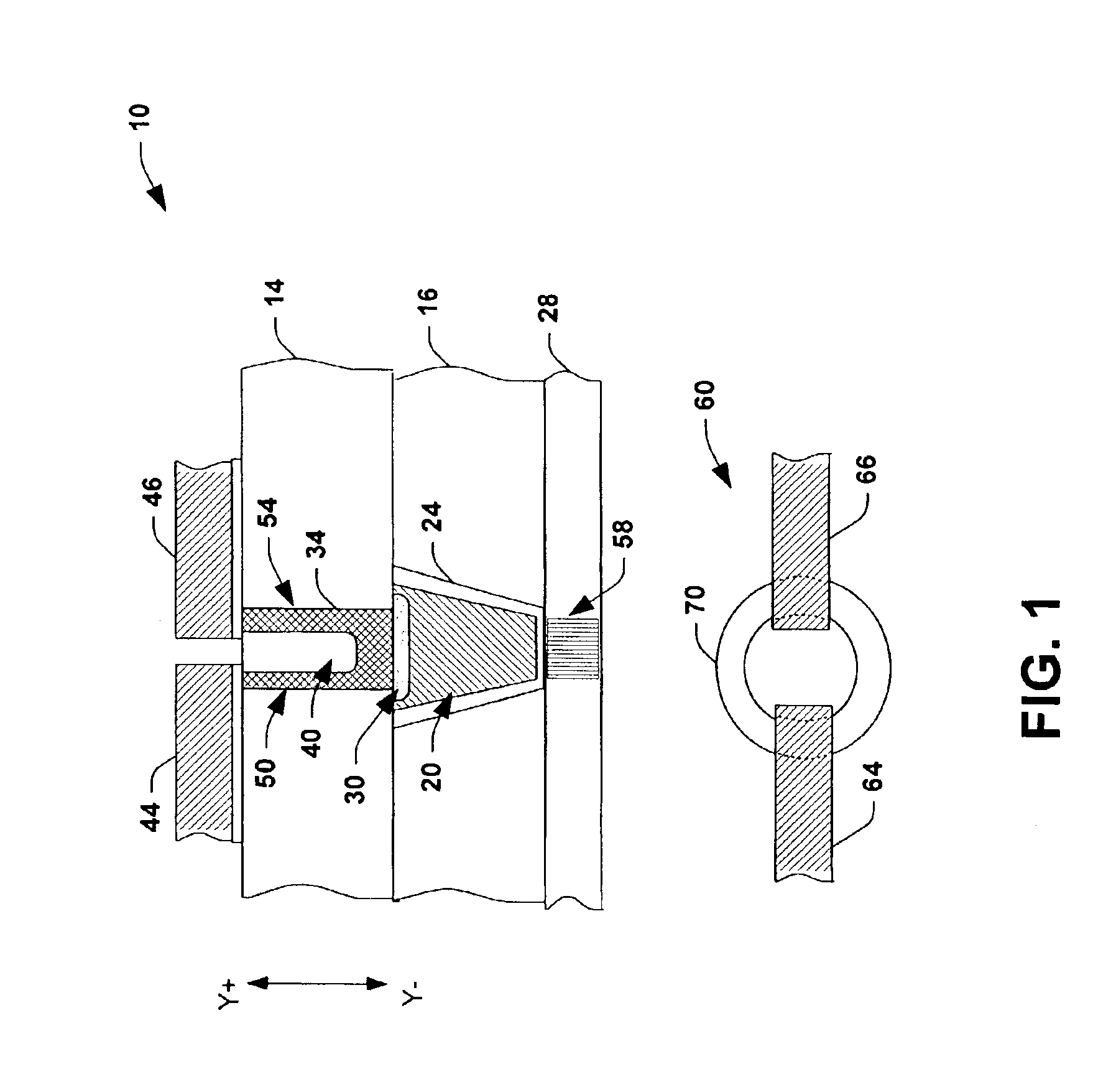
[0026]The present invention provides a multi-cell organic memory device that can operate as a non-volatile memory device having a plurality of multi-cell memory structures constructed within the memory device. A lower electrode can be formed such as from a single or dual damascene process, wherein one or more passive layers are formed on top of the lower electrode. An Inter Layer Dielectric (ILD) is formed above the passive layers and lower electrode, whereby a via or other type relief is created within the ILD and an organic semiconductor material is then utilized to partially fill the via above the passive layer. The portions of the via that are not filled with organic material are filled with dielectric material, thus forming a multi-dimensional memory structure above the passive layer or layers and the lower electrode. One or more top electrodes are then added above the memory structure, whereby distinctive memory cells are created within the organic portions of the memory struc...


PUM

PropertyMeasurementUnit
Digital informationaaaaaaaaaa
Dielectric polarization enthalpyaaaaaaaaaa
Structureaaaaaaaaaa

Abstract

The present invention provides a multi-cell organic memory device that can operate as a non-volatile memory device having a plurality of multi-cell structures constructed within the memory device. A lower electrode can be formed, wherein one or more passive layers are formed on top of the lower electrode. An Inter Layer Dielectric (ILD) is formed above the passive layers and lower electrode, whereby a via or other type relief is created within the ILD and an organic semiconductor material is then utilized to partially fill the via above the passive layer. The portions of the via that are not filled with organic material are filled with dielectric material, thus forming a multi-dimensional memory structure above the passive layer or layers and the lower electrode. One or more top electrodes are then added above the memory structure, whereby distinctive memory cells are created within the organic portions of the memory structure and activated (e.g., read/write) between the top electrodes and bottom electrode, respectively. In this manner, multiple storage cells can be formed within a singular organic structure thereby increasing memory device density and storage.

Description

FIELD OF INVENTION[0001]The present invention relates generally to organic memory devices having polymer films and, in particular, to multi-cell organic memory devices containing an organic semiconductor.BACKGROUND OF THE INVENTION[0002]The volume, use and complexity of computers and electronic devices are continually increasing. Computers consistently become more powerful, new and improved electronic devices are continually developed (e.g., digital audio players, video players). Additionally, the growth and use of digital media (e.g., digital audio, video, images, and the like) have further pushed development of these devices. Such growth and development has vastly increased the amount of information desired / required to be stored and maintained for computer and electronic devices.[0003]Memory devices generally include arrays of memory cells. Each memory cell can be accessed or “read”, “written”, and “erased” with information. The memory cells maintain information in an “off” or an ...

Claims


Application Information

Patent Timeline
IPC IPC(8): H01L51/40H01L51/05H01L51/30H01L27/28H01L51/00
CPCB82Y10/00G11C13/0014G11C13/0016H01L27/285H01L51/0021H01L51/0078H01L51/0035H01L51/0036H01L51/0038H01L51/0041H01L51/0077H01L51/0034H10K19/202H10K71/60H10K85/10H10K85/111H10K85/143H10K85/114H10K85/113H10K85/311H10K85/30
Inventor LOPATIN, SERGEY D.CHANG, MARK S.NGO, MINH VANCHEUNG, PATRICK K.
Owner MONTEREY RES LLC
Why Eureka
Try Eureka