Dual-layer floating gate flexible organic memory device and preparation method therefor

A technology of organic storage devices and floating gates, which is applied in semiconductor/solid-state device manufacturing, electric solid-state devices, semiconductor devices, etc., can solve the problems of device storage reliability decline, reduce leakage current, improve product yield, and excellent heat dissipation The effect of stability and electrical properties

Inactive Publication Date: 2016-05-11
CHINA JILIANG UNIV
View PDF6 Cites 9 Cited by
  • Summary
  • Abstract
  • Description
  • Claims
  • Application Information

AI Technical Summary

Problems solved by technology

However, the requirements for storage density are getting higher and higher. Although the goal can be achieved by increasing the integration level, there are a...

Method used


Image

  • Dual-layer floating gate flexible organic memory device and preparation method therefor

Examples


Embodiment 1

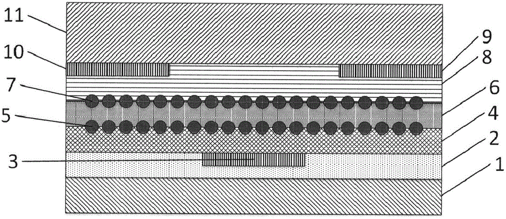
[0026] 1.1 Cut the PET into a 2cm×2.5cm piece, then scrub it with detergent powder, and then use acetone, ethanol, and deionized water to ultrasonically clean it in an ultrasonic cleaner for 10 minutes;

[0027] 1.2 Blow dry 1 under nitrogen, then put it into a vacuum drying oven with a vacuum degree of 0.09Pa, and dry it for 2 hours.

Embodiment 2

[0029] 2.1 Weigh 15mg of purified graphene oxide powder with an electronic scale, weigh 1ml of absolute ethanol with a measuring cylinder, and mix them in a glass bottle;

[0030] 2.2 Seal the bottle and place it on a magnetic stirrer to stir for 1 hour to prepare a 15mg / ml solution;

Embodiment 3

[0032] 3.1 Put the sheet prepared in Example 1 on the suction head of the glue homogenizer, and drop the solution in Example 2 on 1 with a liquid dispenser;

[0033] 3.2 Set the homogenizer at low speed to 300 rpm for 3 seconds, high speed to 1000 rpm for 60 seconds, and start spin coating 2;

[0034] 3.3 After the spin coating is completed, put the sheet into a vacuum drying oven with a vacuum degree of 0.09Pa, a heating temperature of 80°C, and anneal for 2 hours. The thickness of 2 is 20nm after detection by a step meter;


PUM

PropertyMeasurementUnit
Thicknessaaaaaaaaaa
Thicknessaaaaaaaaaa
Thicknessaaaaaaaaaa

Abstract

The invention relates to a dual-layer floating gate flexible organic memory device and a preparation method therefor. The dual-layer floating gate flexible organic memory device mainly comprises a substrate, a dielectric layer, a control gate, a barrier layer, a first floating gate layer, an isolating layer, a second floating gate layer, a tunneling layer, an organic semiconductor layer, a source electrode and a drain electrode, wherein the source electrode and the drain electrode are positioned above the tunneling layer. A dual-layer gold nanocrystalline is taken as the floating gate layers, so that the memory window of the memory device can be improved, and the working voltage range can be expanded; a femtosecond laser reduction technology is adopted, so that a link of intermediate repeated electrode deposition is reduced, the production process is simplified, the pollution doping in the production is lowered, and the product yield can be improved; the barrier layer, the isolating layer and the tunneling layer adopted by the dual-layer floating gate flexible organic memory device all adopt high-dielectric-constant graphene oxide, so that leakage current can be effectively lowered, the stability of the memory can be improved, and the working voltage can be lowered; all the materials adopted by the memory device are flexible and can be bent, so that the memory device can be applied to flexible circuits; and in addition, the femtosecond laser reduction technology and a vacuum thermal evaporation and spin coating technology adopted in the preparation method of the invention are mature in technology and low in product, so that the large-scale production of the dual-layer floating gate flexible organic memory device can be realized.

Description

technical field [0001] The invention relates to the field of semiconductor storage devices, in particular to a double-layer floating gate flexible organic storage device and a preparation method thereof. Background technique [0002] As an important member of non-volatile memory devices, floating gate memory devices have gradually replaced other types of memory due to their high read / write speed, long storage time and service life. Memory cards, U disks, etc. are all based on floating gate storage devices. However, the requirements for storage density are getting higher and higher. Although the goal can be achieved by increasing the integration level, there are also some challenges. The most obvious is that the current leakage caused by the quantum tunneling effect leads to a decrease in the storage reliability of the device. In order to solve the problems encountered, the current main development direction is to replace silicon-based semiconductor materials with organic ma...

Claims


Application Information

Patent Timeline
IPC IPC(8): H01L51/05H01L51/30H01L51/40
CPCH10K85/111H10K10/00H10K10/46
Inventor 唐莹马力超彭应全韦一
Owner CHINA JILIANG UNIV
Why Eureka
Try Eureka