Substrate with transparent conductive layer, and photovoltaic element

a technology of transparent conductive layer and photovoltaic element, which is applied in the manufacture of final products, instruments, lighting and heating apparatus, etc., can solve the problems of increasing the production cost of a single-crystalline silicon photovoltaic element, increasing the manufacturing cost, and increasing the cost of photovoltaic element unit electricity generated compared to an existing power generation method, so as to increase the light absorption in the semiconductor layer, high yield, and high reliability and photoelectric

Inactive Publication Date: 2005-10-04
CANON KK
View PDF4 Cites 50 Cited by
  • Summary
  • Abstract
  • Description
  • Claims
  • Application Information

AI Technical Summary

Benefits of technology

[0030]It is an object of the present invention to solve problems of workability, yield or durability as mentioned above and moreover to increase the light absorption in the semiconductor layer and also pro...

Problems solved by technology

The production cost for a photovoltaic element using such single-crystalline silicon, however, is increased.
Because of a high cost in making silicon wafers and a high manufacturing cost due to the use of a semiconductor process, the photovoltaic element becomes rather expensive for the amount of unit electricity generated compared to an existing power generating method.
It is considered difficult to lower the production cost to a level for power generation.
Thus, in advancement into a practical use for the power source of a photovoltaic element, cost reduction and area increasing are recognized to be important technical problems, and materials that are low in cost or high in conversion efficiency have been searched.
In the above photovoltaic element, however, photoelectric conversion efficiency comparable to that of a photovoltaic element using single-crystalline silicon has not yet been obtained.
Improving the photoelectric conversion efficiency and improving the reliability have been a problem to be studied to make this element practicable as a power element.
One of the important problems in improving the photoelectric conversion efficiency of a film photovoltaic element is to increase the light absorption in a film semiconductor layer and to increase the short-circuit current (Jsc).
When an attempt is made to actually manufacture a photovoltaic element by adopting a back face electrode of such a constitution, several problems appeared from the viewpoint of workability or durability.
First of all, in a semiconductor layer of a pyramid-shaped unevenness having steep vertexes or valleys formed on the surface, a stress is generated locally at the vertex of a pyramid shape and a defect portion is likely to be created in the semiconductor layer.
Besides, when an electromotive force is generated, the leakage current of a photovoltaic element through the defect portion or the like of the semiconductor layer may increase by the concentration of the electric field at the vertex of the pyramid shape, thereby lowering the manufacturing yield of the photovoltaic element.
Furthermore, an increase in the optical degradation (worsening of element characteristics due to long-time light illumination) and the vibrati...

Method used


Image

  • Substrate with transparent conductive layer, and photovoltaic element
  • Substrate with transparent conductive layer, and photovoltaic element
  • Substrate with transparent conductive layer, and photovoltaic element

Examples


example 1

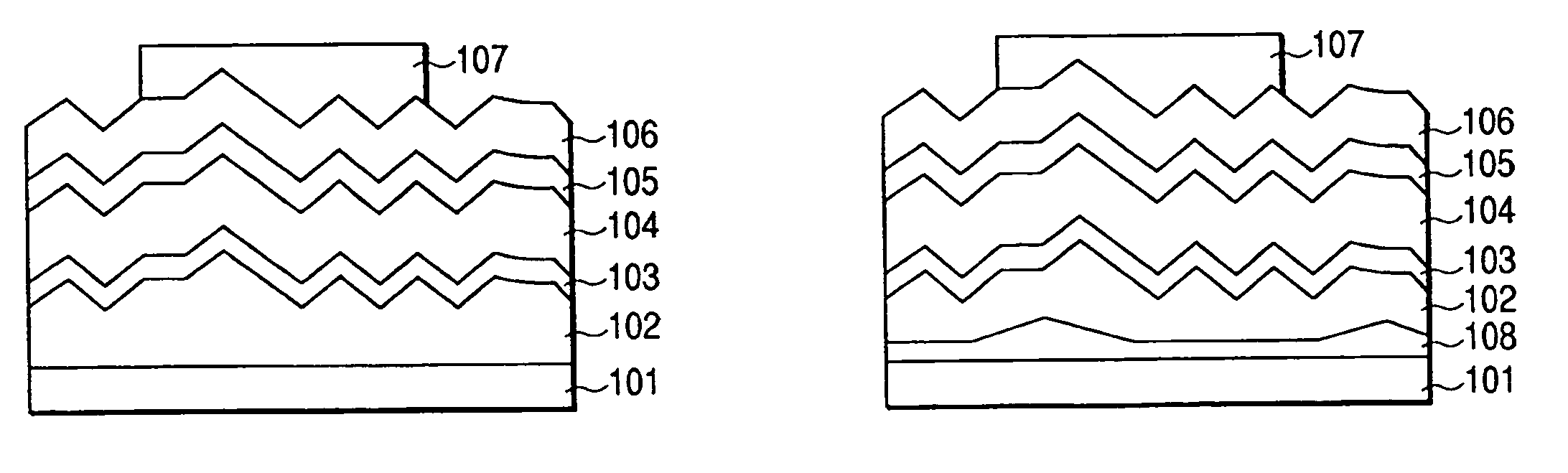
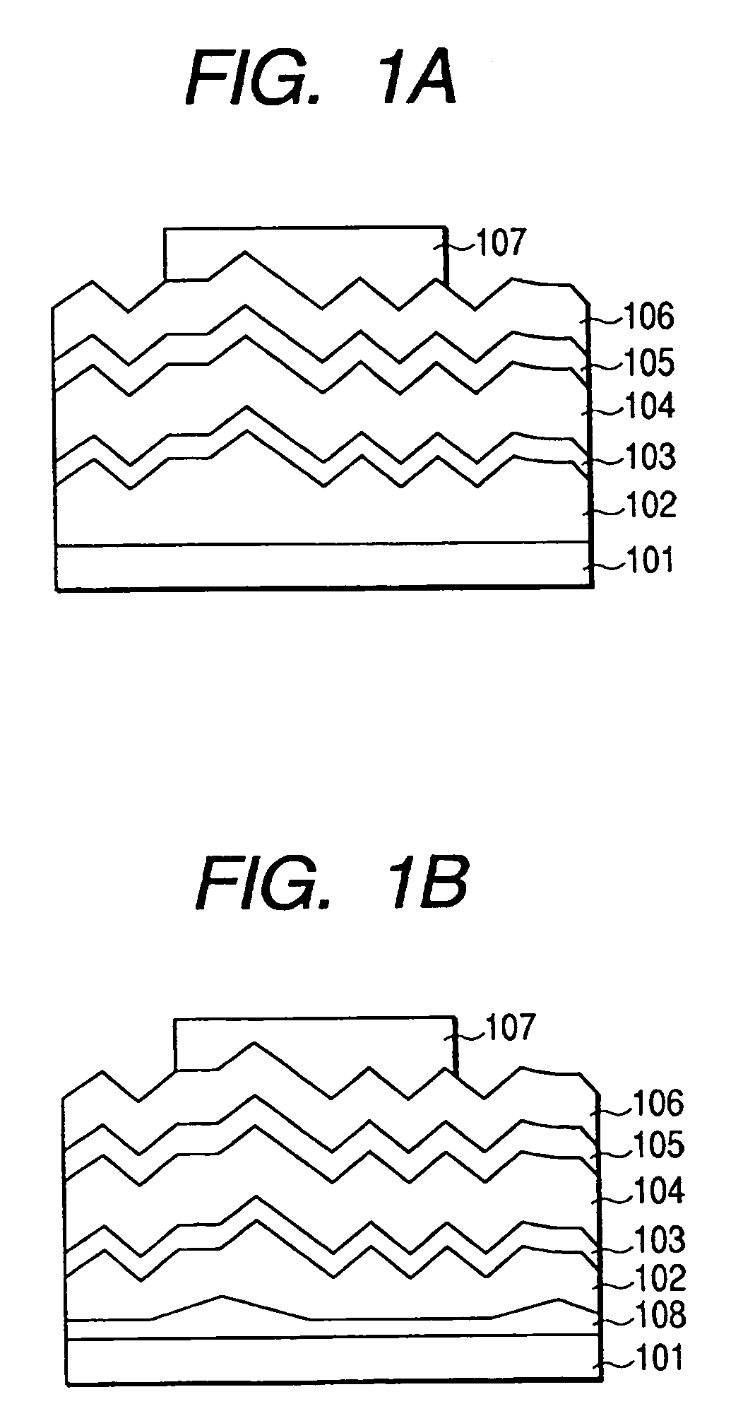
[0170]Initially, a transparent conductive layer 102 was deposited using the depositing apparatus shown in FIG. 3 to prepare a substrate with the transparent conductive layer.

[0171]First, preparation of a supporting substrate 101 was carried out. A 1.1 mm thick, 50×50 mm2 glass substrate (#7059) manufactured by Corning Company was ultrasonically cleaned with acetone and isopropanol and dried by a warm wind.

[0172]To the depositing apparatus shown in FIG. 3, a source gas supply device (not shown in the drawings) is connected through a gas introducing pipe 317. The source gas cylinders, all of which were of ultrahigh purity, comprises an Ar, Xe O2 and F2 gas cylinders. There are targets of Al and ZnO, both of which can be switched for sputtering in vacuum. As the bias power source, an RF power source 311 was used.

[0173]On the substrate holder 302 of FIG. 3, a substrate 303 was placed. Through an exhaust pipe 316 with an oil diffusion pump connected, the depositing chamber 301 was vacuum...

example 2

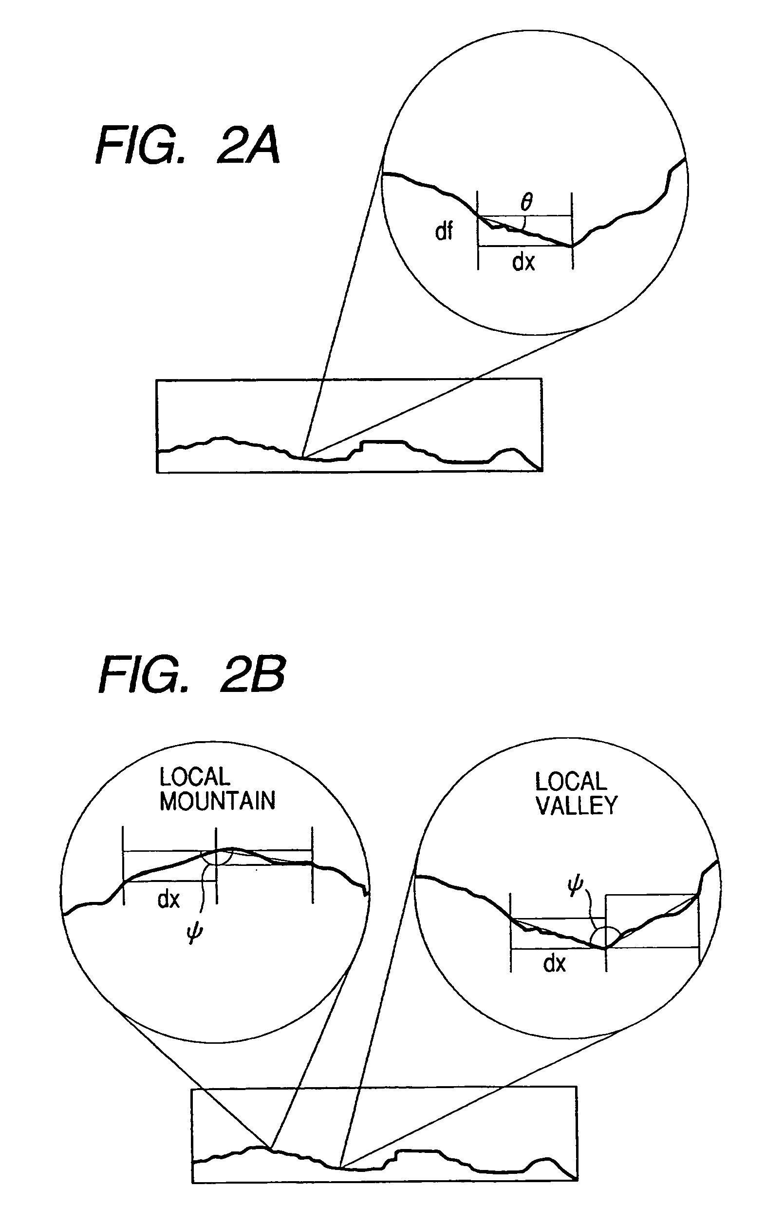
[0190]On a supporting substrate 101 (SUS 304), a 1 μm thick transparent conductive layer 102 having a conductivity of 10−4 (1 / Ωcm) was formed under various conditions by the DC magnetron sputtering process in the same manner as in Example 1. The samples obtained were etched for several seconds in 2% of acetic acid at varied temperatures to prepare various specimens. A distribution of inclinations in the surface was evaluated at a sampling length of 20 nm. The result is shown in Table 4.

[0191]In the same manner as in Example 1, solar cells of pin amorphous silicon semiconductor were produced by stacking the semiconductor layers 103–105. The estimated result is shown in Table 4.

[0192]

TABLE 4AfterReverseAverageAverageBiasKurtosisofofInitialAfterTest atDistri-Standardof Distri-AnglesAnglesConver-AfterVibra-High-SamplingbutionDeviationbutionininConduc-sionOpticaltionalTemperatureTotalLengthof Incli-of Incli-of Incli-LocalLocaltivityEffi-Deterio-Deterio-and High-Estima-Sample No.(nm)natio...

example 3

[0193]On a supporting substrate 101 (SUS 304), a 1 μm thick transparent conductive layer 102 having a conductivity of 10−4 (1 / Ωcm), made of a tin oxide film, was formed under various conditions by the magnetron sputtering process in accordance with a forming method similar to that of Example 1.

[0194]An estimate was made with the standard deviation of inclinations of 30°±2°. The average of angles in local valleys of the surface was evaluated. The result is shown in Table 5.

[0195]In the same manner as in Example 1, solar cells of pin amorphous silicon semiconductor were produced by stacking the semiconductor layers. At that time, the deposition speed of the i-type semiconductor layer 104 was increased to 20 Å / s. The estimated result is shown in Table 5.

[0196]

TABLE 5AfterReverseAverageAverageBiasKurtosisofofInitialAfterTest atDistri-Standardof Distri-AnglesAnglesConver-AfterVibra-High-SamplingbutionDeviationbutionininConduc-sionOpticaltionalTemperatureTotalSampleLengthof Incli-of Incli...


PUM

PropertyMeasurementUnit
Angleaaaaaaaaaa
Angleaaaaaaaaaa
Angleaaaaaaaaaa

Abstract

The present invention provides a substrate with a transparent conductive layer comprising at least one layer stacked on a supporting substrate, wherein the surface of the transparent conductive layer has a distribution of inclination arctan (df/dx) in the range of sampling length dx between 20 nm and 100 nm when a distance of the surface of said transparent conductive layer from the surface of said supporting substrate is regarded as f being a normal distribution having a kurtosis of −1.2 to 0.5 around 0° and a standard deviation of 20° to 55°, and a photovoltaic element using the substrate. The substrate can be produced at a high yield and a low cost suitable for practical use and has a high reliability. In addition, a photovoltaic element having a high photoelectric conversion efficiency is obtained when the substrate is used in manufacturing it.

Description

BACKGROUND OF THE INVENTION[0001]1. Field of the Invention[0002]The present invention relates to a substrate with transparent conductive layer(s), more particularly a substrate for a photovoltaic element with transparent conductive layer(s) capable of improving the yield in the production process and reliability such as weatherability or durability while improving the efficiency of photoelectric conversion by use of light confinement effect, and a photovoltaic element using the same. The photovoltaic element is one used for solar cells, photodiodes, electrophotographic photosensitive materials or the like.[0003]2. Related Background Art[0004]A photovoltaic element for converting light into electric energy has been widely applied to a small power source for public appliances, such as electronic calculators or wrist watches, as a solar cell and attracts attention as a technique practicable for future substitutes to so-called fossil fuels such as petroleum and coal. It is also used for...

Claims


Application Information

Patent Timeline
IPC IPC(8): B32B9/04H01L31/0224H01L31/0236H01L31/0392H01L31/052H01L31/075H01L31/20
CPCH01L31/022466H01L31/0236H01L31/0392H01L31/03921H01L31/056H01L31/202H01L31/075Y02E10/548Y02E10/52H01L31/022475H01L31/022483H01L31/02363H01L31/02366H01L31/03923H01L31/03925Y02E10/541Y02P70/50
Inventor HIGASHIKAWA, MAKOTO
Owner CANON KK
Why Eureka
Try Eureka