Solid material comprising a thin metal film on its surface and methods for producing the same

a technology of solid materials and metal films, which is applied in the direction of vacuum evaporation coatings, coatings, chemical vapor deposition coatings, etc., can solve the problems of pin holes, gaps and/or defects on the surface, and uneven thickness of metal film thin films,

Inactive Publication Date: 2005-10-25
UNIV TECH
View PDF11 Cites 119 Cited by
  • Summary
  • Abstract
  • Description
  • Claims
  • Application Information

AI Technical Summary

Benefits of technology

[0019]A solid material produced by the present methods comprises a thin metal film layer, wherein the ratio of roughness of the solid substrate surface to roughness of the solid material surface with the thin metal film layer is from about 0.8 to about 1.2, preferably from about 0.9 to about 1.2, and more preferably from about 1 to about 1.2.
[0020]The roughness of a flat portion of the solid material is about 50% or less of roughness of a substantially same solid material produced by a chemical vapor deposition process or 50% or less of roughness of a substantially same solid material in a ballistic deposition model, preferably the roughness is about 40% or less, and more preferably about 30% or less. This percentage is expected to decrease as the thickness increases. The roughness of solid material produced by the present method should be substantially constant independent of the film thickness. In contrast, the roughness of the solid material produced by the CVD will generally depend on the square root of the thickness.
[0021]As stated above, while a variety of metal film thickness can be achieved by the methods of the present invention, a solid material having a tungsten film layer thickness of about 100 Å or less, preferably 50 Å or less, are particularly useful in a variety of electronic application. For a solid material having a tungsten film, the thickness of the tungsten film layer is substantially equal to 2.5 Å×n, where n is an integer and represents the number of complete cycles of the plurality of self-limiting reactions.

Problems solved by technology

However, the CVD process often results in pin-holes, gaps and / or defects on the surface.
Furthermore, the resulting thin metal film surface is often rough and has uneven metal film thickness.
While thin films of a variety of binary materials can be grown with atomic layer control using sequential self-limiting surface reactions [5,6], thin film of metal using ALD has not been successful achieved.
In contrast, the atomic layer growth of single-element, e.g., metal, films has never been achieved using this approach.
Earlier efforts to deposit copper with atomic layer control were unsuccessful because the surface chemistry was not self-limiting and the resulting copper films displayed coarse polycrystalline grains [17,18].
Previous attempts to achieve silicon ALD with sequential surface chemistry could not find a set of reactions that were both self-limiting [19].

Method used


Image

  • Solid material comprising a thin metal film on its surface and methods for producing the same
  • Solid material comprising a thin metal film on its surface and methods for producing the same
  • Solid material comprising a thin metal film on its surface and methods for producing the same

Examples


experimental 1

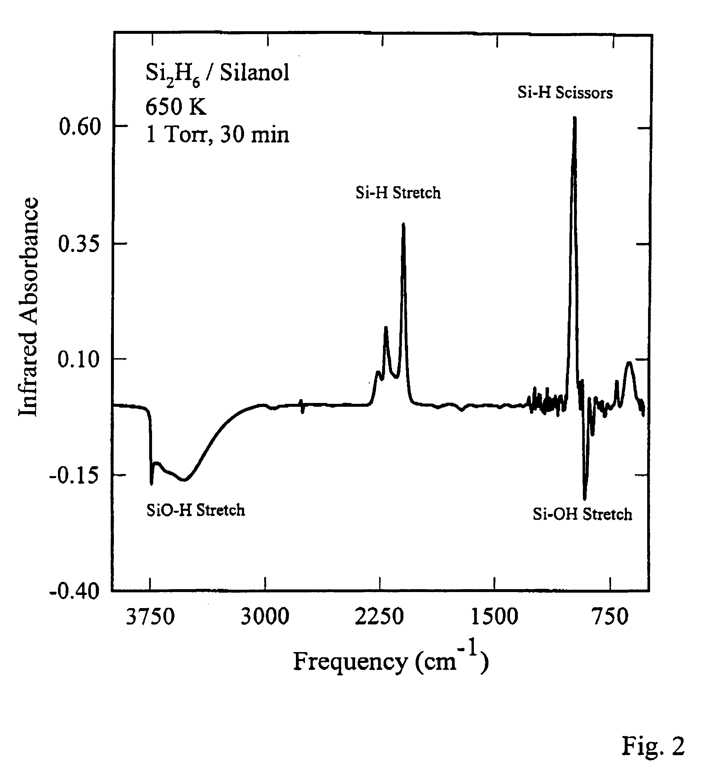
[0056]This experiment is directed to FTIR Spectroscopy Studies of Silica Powder.

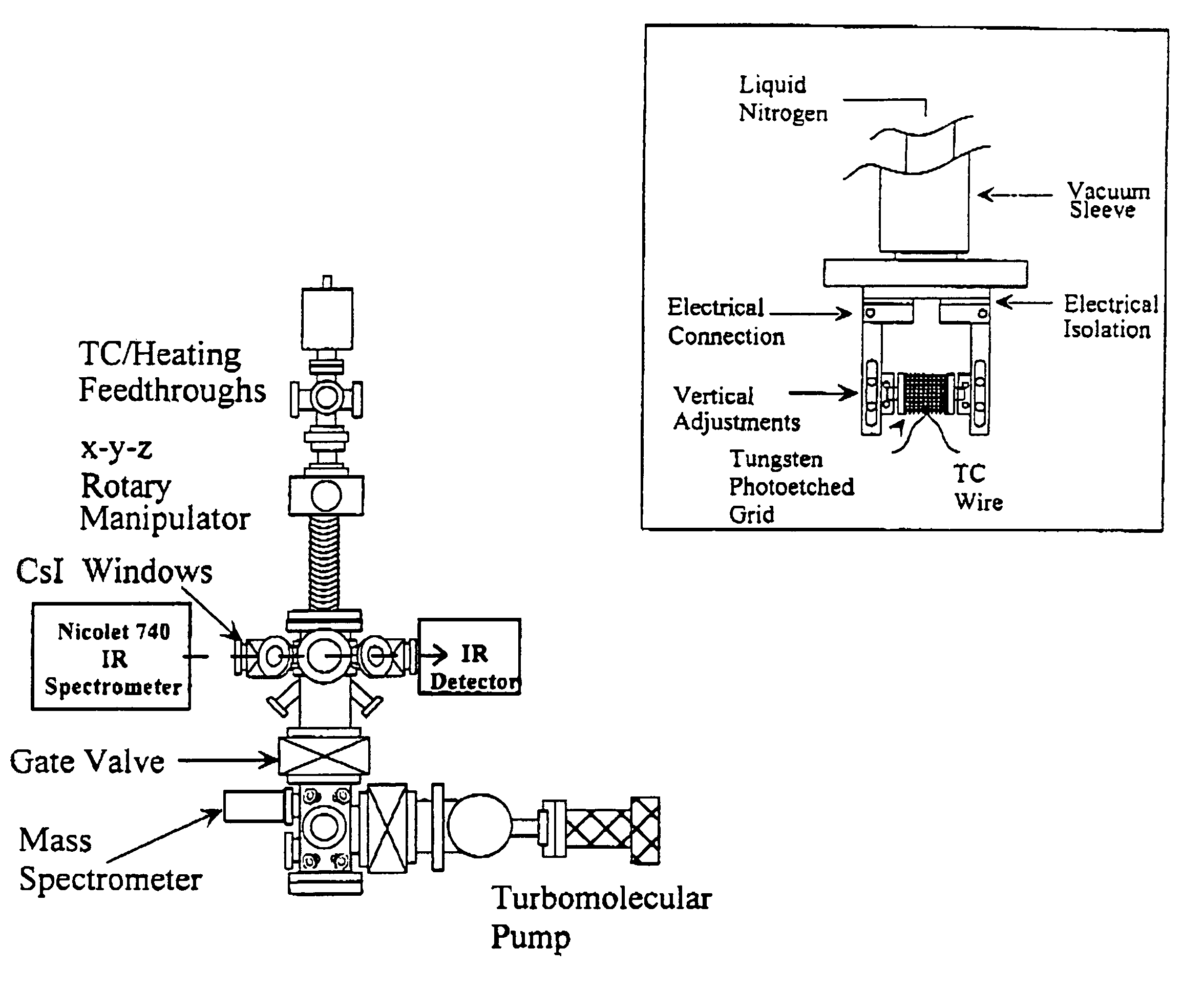
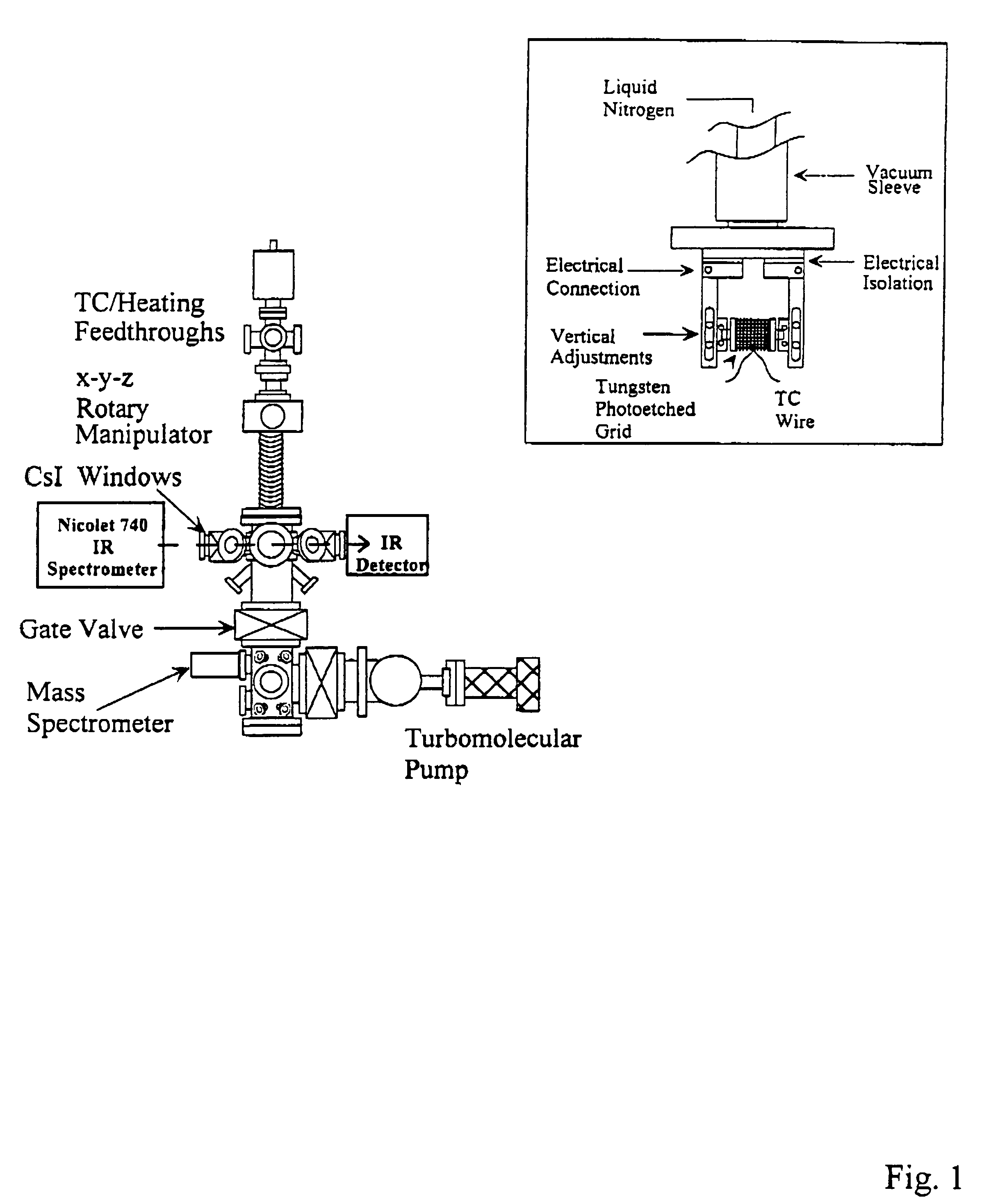
[0057]The FTIR spectroscopy experiments were performed in a high vacuum chamber built for in situ transmission FTIR spectroscopic investigations [27]. A schematic of this chamber is displayed in FIG. 1. The chamber was equipped with a 200 L / s turbomolecular pump, CsI windows, an ion gauge, a capacitance manometer, and a quadrupole mass spectrometer. The chamber had a base pressure of 5×10⁻⁸ Torr. The vibrational spectra were recorded with a Nicolet 740 FTIR spectrometer using an MCT-B detector.

[0058]High surface area silica powder was used to achieve sufficient surface sensitivity for the FTIR investigations. High surface area fumed silica powder was obtained from Aldrich. This silica powder had a surface area of 380 m2 / g. The silica powder was pressed into an tungsten photoetched grid [28]. This tungsten grid from Buckbee-Mears was 0.002 inch thick and contained 100 lines per inch. The tungsten was then...

experiment 2

[0062]This experiment is directed to Spectroscopic Ellipsometry Studies of Si(100).

[0063]The tungsten film growth experiments were performed in a high vacuum apparatus designed for ellipsometric investigations of thin film growth [7]. A schematic of this apparatus is shown in FIG. 3. The apparatus consists of a sample load lock chamber, a central deposition chamber and a ultra high vacuum chamber for surface analysis. The central deposition chamber is capable of automated dosing of molecular precursors under a wide variety of conditions. The deposition chamber is pumped with either a 175 L / s diffusion pump backed by a liquid N2 trap and a mechanical pump or two separate liquid N2 traps backed by mechanical pumps. This chamber had a base pressure of 1×10⁻⁷ Torr.

[0064]The central deposition chamber is equipped with an in situ spectroscopic ellipsometer (J. A. Woolam Co. M-44). This ellipsometer collects data at 44 visible wavelengths simultaneously. The ellipsometer is mounted on port...


PUM

PropertyMeasurementUnit
temperatureaaaaaaaaaa
vapor pressureaaaaaaaaaa

Abstract

The present invention provides a solid material comprising a solid substrate having a thin metal film and methods for producing the same. The method generally involves using a plurality self-limiting reactions to control the thickness of the metal film.

Description

CROSS-REFERENCE TO RELATED APPLICATIONS[0001]This application claims the benefit of U.S. Provisional Application No. 60 / 124,532, filed Mar. 15, 1999.STATEMENT REGARDING FEDERALLY SPONSORED RESEARCH OR DEVELOPMENT[0002]The U.S. Government has a paid-up license in this invention and the right in limited circumstances to require the patent owner to license others on reasonable terms as provided for by the terms of Grant No. DAAG55-98-C-0036 awarded by DARPA, in conjunction with the U.S. Army Research Office and by the terms of a Grant No. F49620-99-1-0081 by Air Force Office of Scientific Research.BACKGROUND OF THE INVENTION[0003]The atomic layer controlled growth or atomic layer deposition (ALD) of single-element films is important for thin film device fabrication [1]. As component sizes shrink to nanometer dimensions, ultrathin metal films are necessary as diffusion barriers to prevent interlayer and dopant diffusion [2]. Conformal metal films are needed as conductors on high aspect ...

Claims


Application Information

Patent Timeline
Patent Type & Authority Patents(United States)
IPC IPC(8): C23C16/00C23C14/00C23C16/08C23C16/44C23C16/455
CPCC23C16/08C23C16/45525
Inventor KLAUS, JASON W.GEORGE, STEVEN M.
Owner UNIV TECH
Why Eureka
Try Eureka