N-channel LDMOS with buried p-type region to prevent parasitic bipolar effects

Inactive Publication Date: 2005-10-25
TEXAS INSTR INC
View PDF4 Cites 83 Cited by
  • Summary
  • Abstract
  • Description
  • Claims
  • Application Information

AI Technical Summary

Benefits of technology

[0016]The disclosed structure not only collects secondary holes efficiently, but also reduces the base resistance and hence the base-emitter volt

Problems solved by technology

A transistor loaded only by a pure resistance will have only one line of voltage/current values for a given gate voltage, but in real-world applications the operating point can also be affected by the load's reactive and/or hysteretic characteristics.
Thus movement within the SOA occurs as the LDMOS interacts with the circuit, and there is a risk that switching transients can lead to current/voltage trajectories that cross the boundary of the SOA.
A transistor in this state is likely to destroy itself or its power supply connections.
SOA performance is a particular problem for N-channel Ldmos transistors.
However, a drawback of the n-Ldmos is that its safe operating area is generally inferior to that of a p-Ldmos.
The negative resistance and snapback behavior are due to the presence of th

Method used


Image

  • N-channel LDMOS with buried p-type region to prevent parasitic bipolar effects
  • N-channel LDMOS with buried p-type region to prevent parasitic bipolar effects
  • N-channel LDMOS with buried p-type region to prevent parasitic bipolar effects

Examples


Embodiment Construction

[0031]The numerous innovative teachings of the present application will be described with particular reference to the presently preferred embodiment. However, it should be understood that this class of embodiments provides only a few examples of the many advantageous uses of the innovative teachings herein. In general, statements made in the specification of the present application do not necessarily delimit any of the various claimed inventions. Moreover, some statements may apply to some inventive features but not to others.

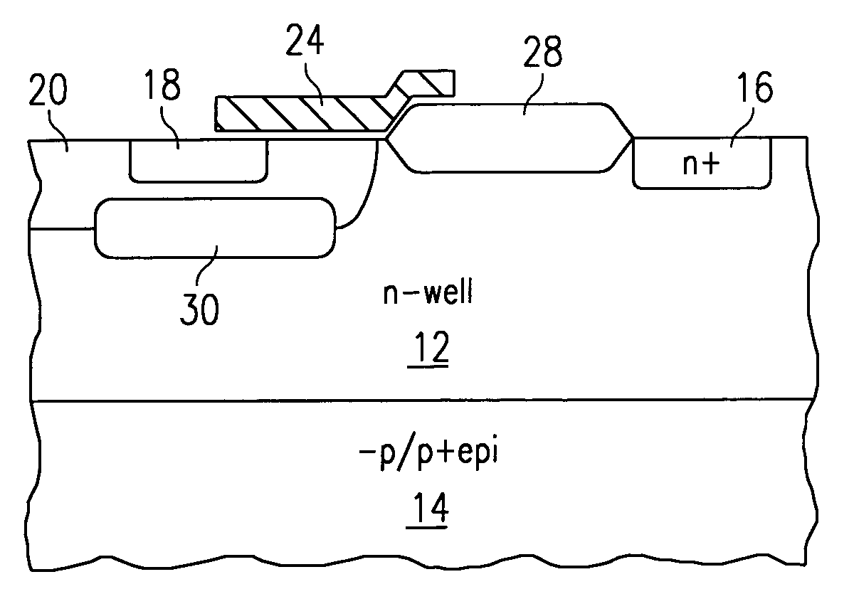
[0032]FIG. 1 is a conceptual cross-section of a sample embodiment of the inventive LDMOS transistor. (This embodiment is an n-channel LDMOS transistor—since n-channel is particularly advantageous due to the difference in impact ionization coefficients mentioned above—but the disclosed principles can also be adapted, less advantageously, to a p-channel device.) The transistor 10 is formed in a semiconductor starting structure 14 with the drain region 16 located ...


PUM


Abstract

An improved n-channel integrated lateral DMOS (10) in which a buried body region (30), beneath and self-aligned to the source (18) and normal body diffusions, provides a low impedance path for holes emitted at the drain region (16). This greatly reduces secondary electron generation, and accordingly reduces the gain of the parasitic PNP bipolar device. The reduced regeneration in turn raises the critical field value, and hence the safe operating area.

Description

CROSS-REFERENCE TO OTHER APPLICATION[0001]This application claims priority form provisional 60 / 259,322 filed Dec. 31, 2000, which is hereby incorporated by reference.BACKGROUND AND SUMMARY OF THE INVENTION[0002]The present invention relates to integrated circuit structures and fabrication methods, and more particularly to smart power structures which include n-channel lateral DMOS as well as logic transistors.Background: DMOS and LDMOS[0003]DMOS devices are “double diffused” metal oxide semiconductor (MOS) field effect transistors, or MOSFETs. DMOS are power devices which can be used as individual devices or as components within power integrated circuits. A DMOS is characterized by a source region and a body (or backgate) region which are simultaneously diffused, so that the transistor's channel length is defined by the difference between two diffusion lengths, rather than by separate a patterned dimension. The double-diffusion structure of the DMOS transistor enables a short channe...

Claims


Application Information

Patent Timeline
IPC IPC(8): H01L21/336H01L29/66H01L21/02H01L29/10H01L29/78H01L29/02H01L29/40H01L29/45H01L29/08H01L27/085H01L29/417H01L29/423
CPCH01L29/0878H01L29/1095H01L29/66689H01L29/7816H01L29/41766H01L29/42368H01L29/456H01L27/085
Inventor HOWER, PHILIP L.EFLAND, TAYLOR R.
Owner TEXAS INSTR INC
Why Eureka
Try Eureka