
Method to monitor and control the crystal cooling or quenching rate by measuring crystal surface temperature

a technology of crystal surface temperature and temperature measurement, which is applied in the direction of crystal growth process, polycrystalline material growth, crystal growth process, etc., can solve the problems of agglomeration intrinsic point defects, edge slippage, and the number of defects in single crystal silicon form, and achieve the effect of facilitating the growth of ingots

Inactive Publication Date: 2005-11-01
SUNEDISON SEMICON LIMITED UEN201334164H
View PDF7 Cites 2 Cited by
  • Summary
  • Abstract
  • Description
  • Claims
  • Application Information

AI Technical Summary

Benefits of technology

"The present invention provides a method and apparatus for growing high-quality monocrystalline ingots using the Czochralski method with reduced defects. The invention includes a crystal puller and method for growing ingots with reduced agglomerated defects. Additionally, the invention includes a system for monitoring the thermal history of the ingot during or post growth processing to adjust processing parameters in real-time to achieve an optimal cooling rate without generating edge slips. The technical effects of the invention include improved quality and efficiency of monocrystalline ingots and reduced defects during production."

Problems solved by technology

It is now recognized that a number of defects in single crystal silicon form in the growth chamber as the post growth ingot cools from the temperature of solidification.
Upon cooling to below this threshold temperature, a reaction or agglomeration event occurs, resulting in the formation of agglomerated intrinsic point defects, which can produces other defects such as edge slips.
Such defects are not responsible for gate oxide integrity failures, an important wafer performance criterion, but they are widely recognized to be the cause of other types of device failures usually associated with current leakage problems.
First, defect “nucleation” occurs, which is the result of the intrinsic point defects being supersaturated at a given temperature.
Below the second threshold temperature, intrinsic point defects are no longer mobile within commercially practical periods of time.
While the ingot remains above this temperature, vacancy or interstitial intrinsic point defects diffuse through the crystal lattice to sites where agglomerated vacancy defects or interstitial defects, respectively, are already present, causing a given agglomerated defect to grow in size.
Reducing the quenching rate too severely can compromise process robustness in production.
For example, production yield loss has been identified to be caused by insufficient cooling.
However, pulling the post growth ingot according to a predetermined fixed rate does not allow adjustments for temperature variations, which frequently occur during post growth cooling stages in almost all of the crystal processes.

Method used


Image

  • Method to monitor and control the crystal cooling or quenching rate by measuring crystal surface temperature
  • Method to monitor and control the crystal cooling or quenching rate by measuring crystal surface temperature
  • Method to monitor and control the crystal cooling or quenching rate by measuring crystal surface temperature

Examples


Embodiment Construction

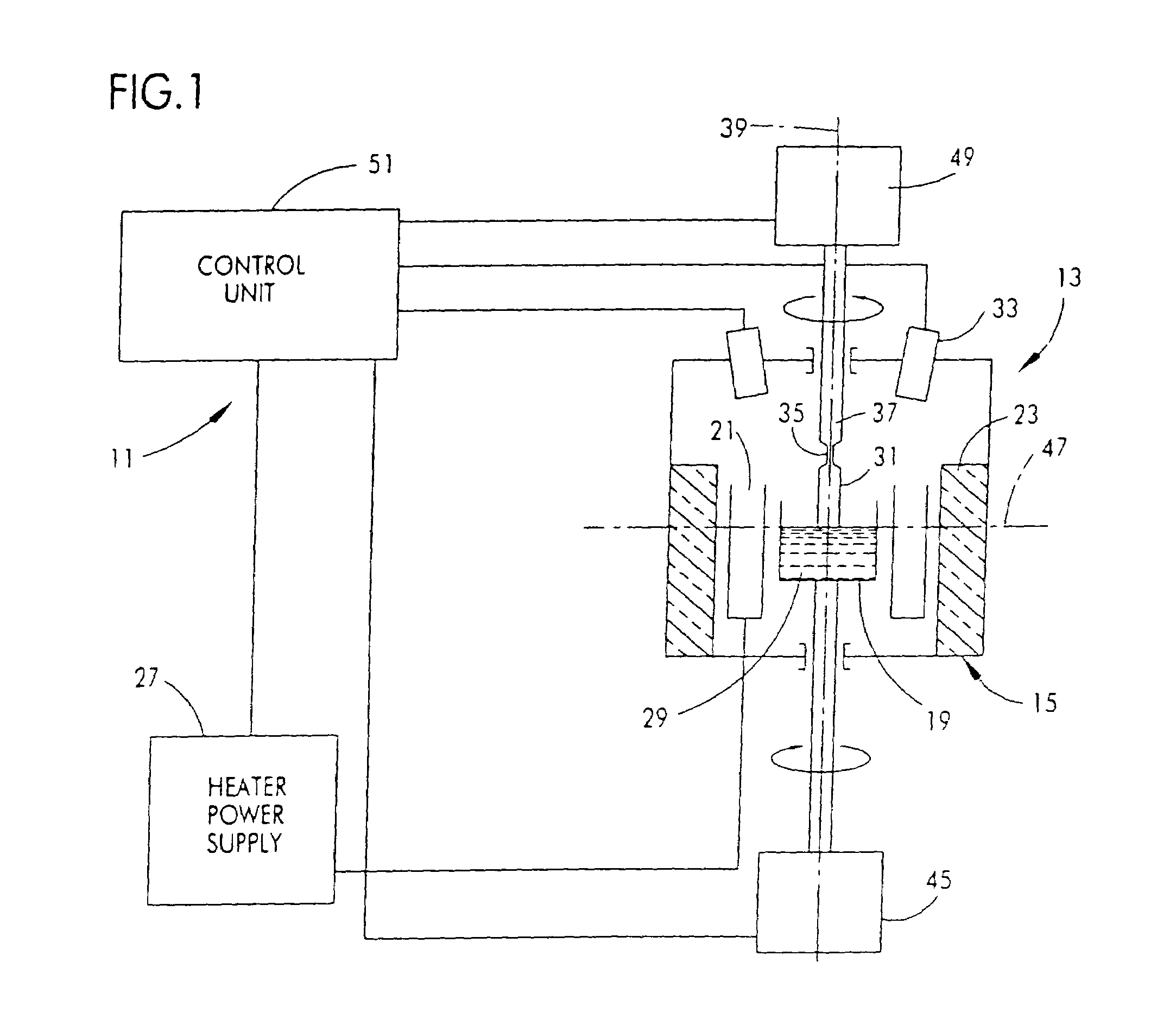
[0030]Referring now to FIG. 1, a system, indicated generally at 11, is shown for use with a Czochralski crystal growing apparatus, indicated generally at 13. The details of construction of the crystal growing apparatus 13 are well known to those of ordinary skill in the art. In general, crystal growing apparatus 13 includes a vacuum chamber 15 enclosing a crucible 19. Heating means such as a resistance heater 21 surrounds the crucible 19. In one embodiment, insulation 23 lines the inner wall of vacuum chamber 15 and a chamber cooling jacket (not shown) fed with water surrounds it. A vacuum pump (not shown) typically removes gas from within the vacuum chamber 15 as an inert atmosphere of argon gas is fed into it.

[0031]According to the Czochralski single crystal growth process, a quantity of polycrystalline silicon, or polysilicon, is charged to crucible 19. A heater power supply 27 provides electric current through the resistance heater 21 to melt the charge and, thus, form a silicon...


PUM

PropertyMeasurementUnit
temperatureaaaaaaaaaa

Abstract

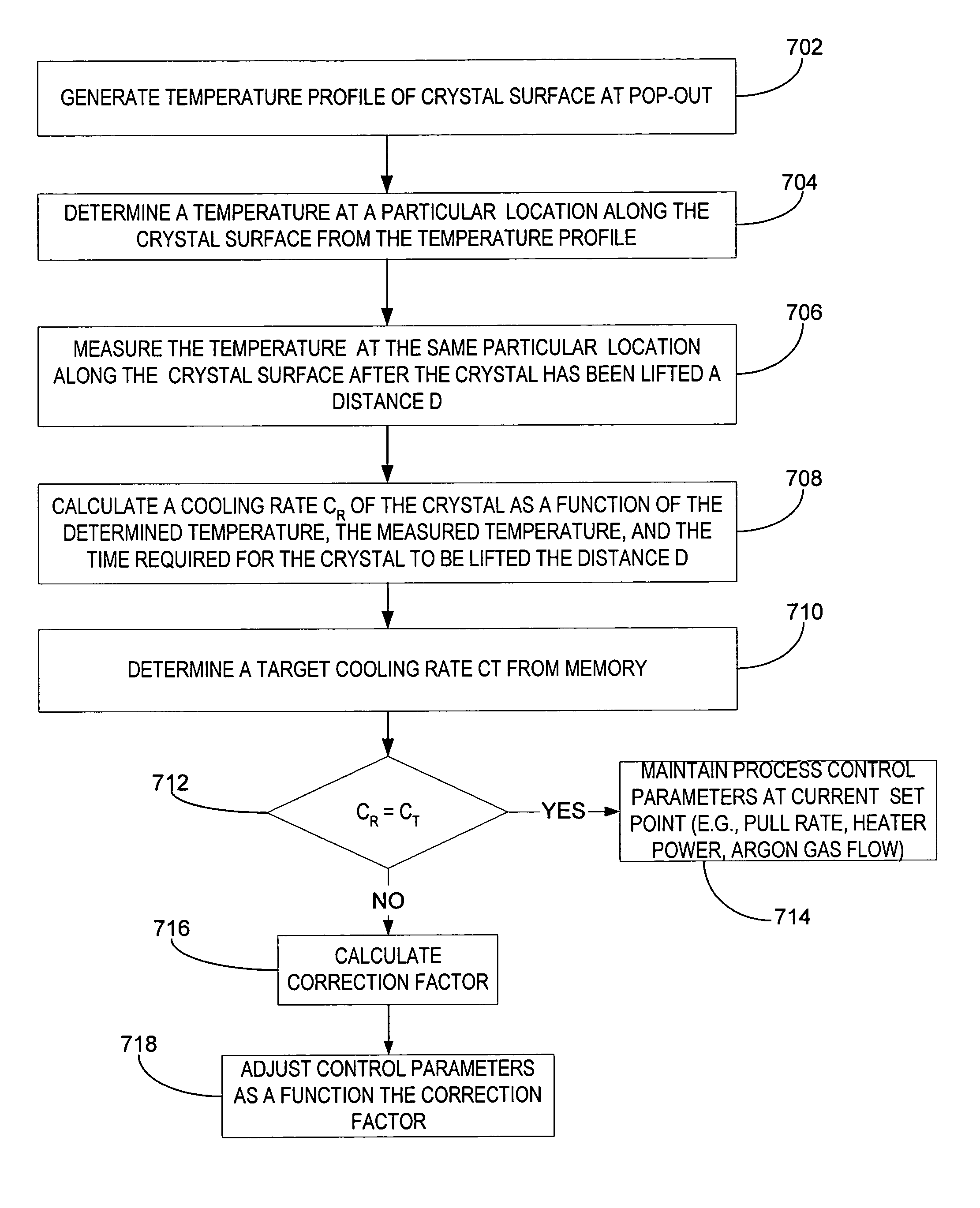
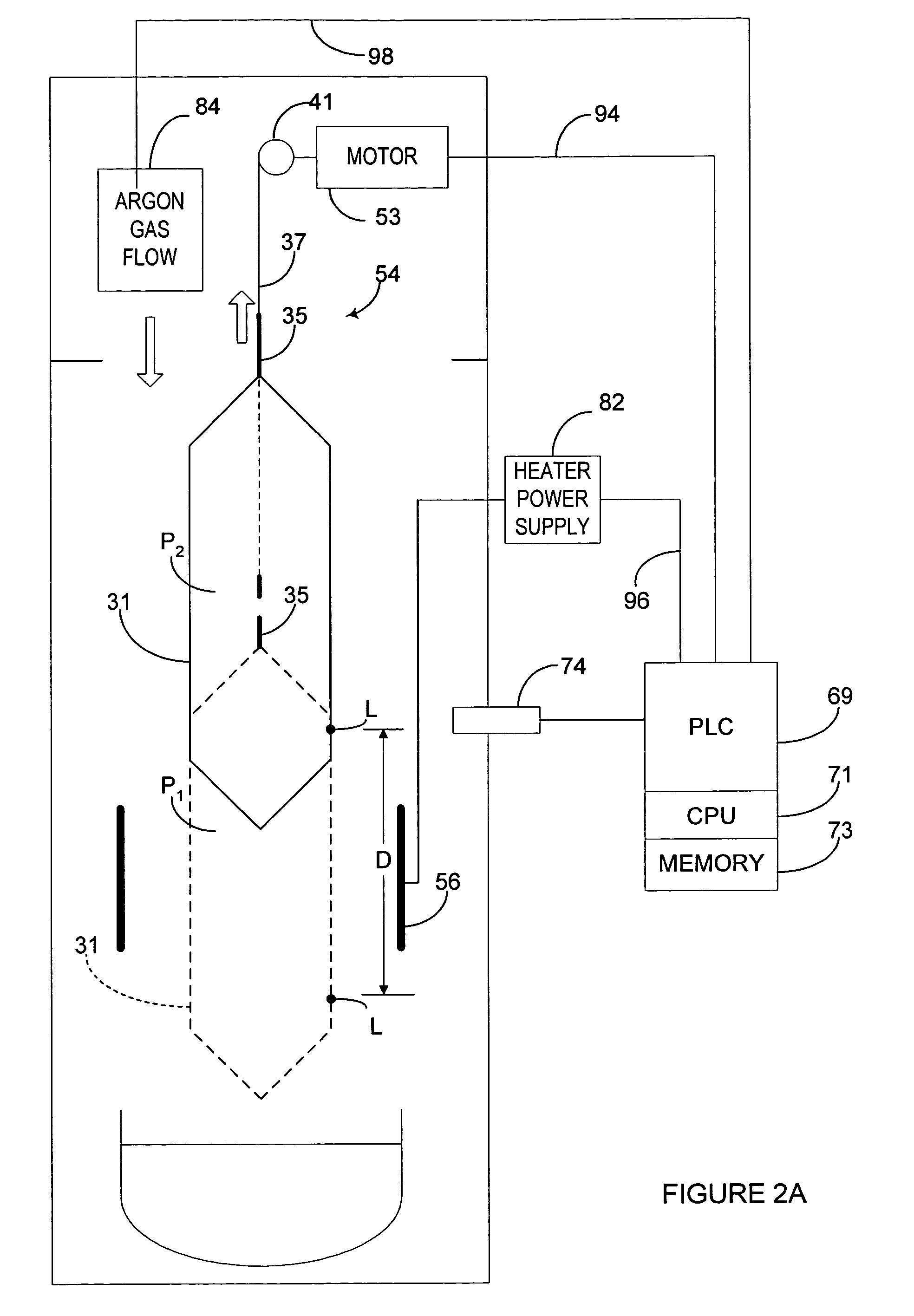
A method and apparatus for controlling the quenching rate of a monocrystalline ingot pulled from a melt by adjusting one or more post growth processing parameter. A temperature model generates a temperature profile that represents the surface temperature along the length of the ingot at the instant it is pulled from the melt. A first temperature at a particular location along the length of the crystal is determined from the temperature profile. A temperature sensor senses a second temperature at the same particular location. A PLC calculates a quenching rate of the crystal as a function of the first temperature and the second temperature. The PLC generates an error between a target quenching rate and a calculated quenching rate, and one or more post growth process parameters are adjusted as function of the error signal to optimize the quenching rate. Alternatively, temperature readings from the sensor are collected and the quenching rates of the crystal are calculated after crystal growth and post growth quenching. One or more post growth process parameters are modified and programmed for subsequent crystal growth and post growth quenching to achieve optimized quenching rate and crystal quality.

Description

BACKGROUND OF THE INVENTION[0001]The present invention relates generally to crystal growing apparatus used in growing monocrystalline silicon ingots, and more particularly to a control assembly for use in such a crystal growing apparatus. Single crystal silicon, which is the starting material for most semiconductor electronic component fabrication, is commonly prepared by the so-called Czochralski (“Cz”) method. Conventional growth of the crystal is most commonly carried out in a crystal pulling furnace. In this method, polycrystalline silicon (“polysilicon”) is charged to a crucible and melted by a heater surrounding the outer surface of the crucible side wall. A seed crystal is brought into contact with the molten silicon and a single crystal ingot is grown by relatively slow extraction via a crystal puller. After formation of a neck is complete, the diameter of the crystal ingot is enlarged by decreasing the pulling rate and / or the melt temperature until the desired or target dia...

Claims


Application Information

Patent Timeline
Patent Type & Authority Patents(United States)
IPC IPC(8): C30B35/00C30B15/20C30B29/06
CPCC30B15/20C30B29/06C30B35/00Y10T117/1008Y10T117/1004Y10T117/1032
Inventor LU, ZHENGKIMBEL, STEVEN L.
Owner SUNEDISON SEMICON LIMITED UEN201334164H
Learn More