Photoelectric conversion device

Active Publication Date: 2005-11-01
CANON KK
View PDF8 Cites 177 Cited by
  • Summary
  • Abstract
  • Description
  • Claims
  • Application Information

AI Technical Summary

Benefits of technology

[0007]An object of the present invent

Problems solved by technology

However, in the aforementioned photoelectric conversion device of the conventional art, there are problems described below.
This through-current reduces voltage on a power supply path or a ground potential supply path to cause flu

Method used


Image

  • Photoelectric conversion device
  • Photoelectric conversion device
  • Photoelectric conversion device

Examples


Example

[0021]First Embodiment

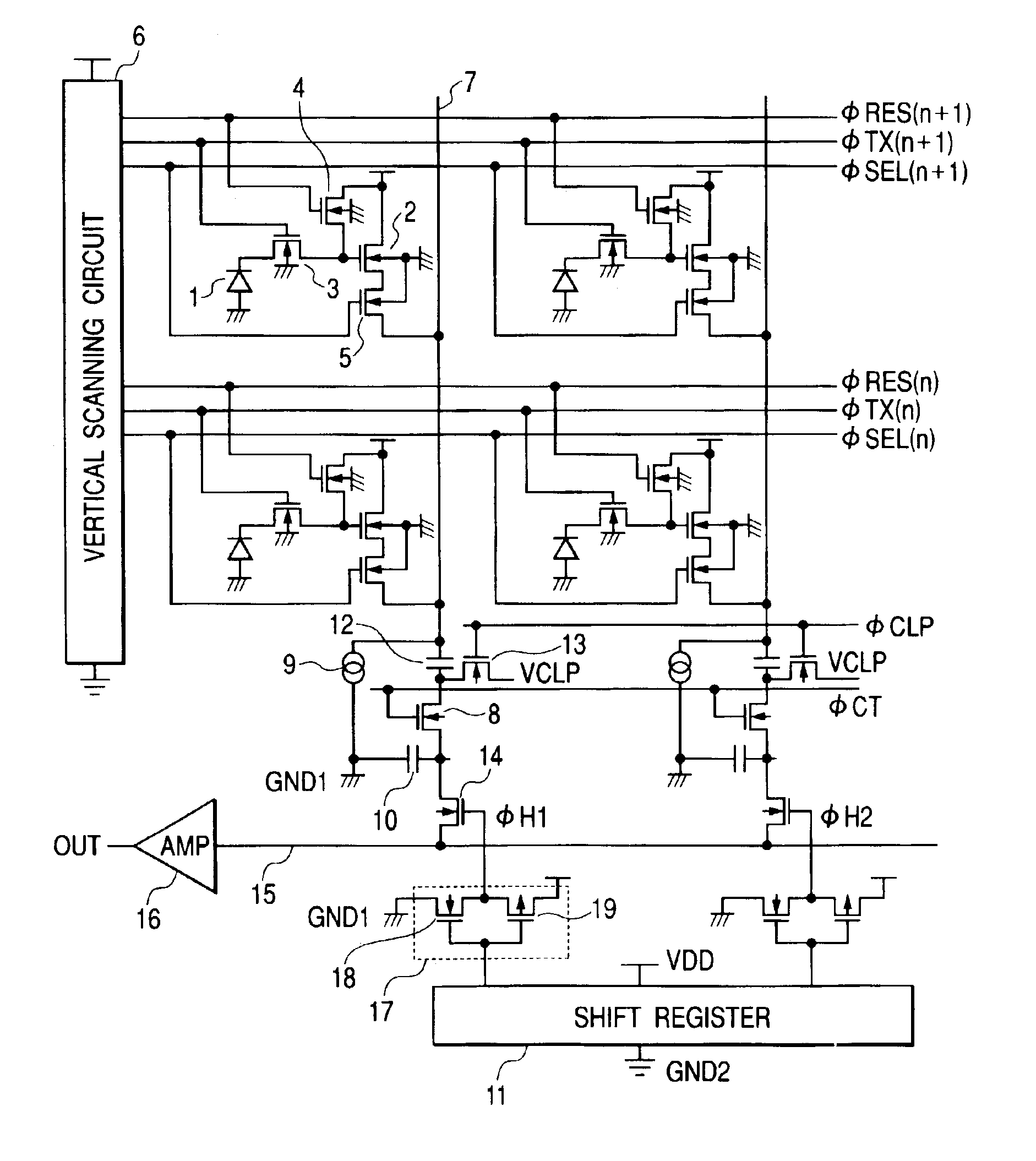
[0022]The first embodiment of the present invention will be described in detail. FIG. 1 is a conceptual diagram showing an equivalent circuit of a photoelectric conversion device of the first embodiment. This photoelectric conversion device is formed on a single semiconductor substrate by, for example a CMOS process.

[0023]In the drawing, pixels are arranged in 2×2 array in horizontal and vertical directions, but the pixels are not particularly limited to this array. In FIG. 1, a unit pixel includes a photodiode 1 which is a photoelectric conversion element, an amplification metal oxide semiconductor field effect transistor (MOSFET) 2 for amplifying a signal generated by the photodiode 1, a reset switch 4 for resetting an input of the amplification MOSFET 2 to predetermined voltage, and a select switch 5 for controlling electrical connection between a source electrode of the amplification MOSFET 2 and a vertical output line 7. Additionally, a transfer switch 3 i...

Example

[0040]Second Embodiment

[0041]The second embodiment of the present invention will be described in detail. FIG. 4 is a conceptual diagram showing an equivalent circuit of a photoelectric conversion device of the second embodiment. The photoelectric conversion device shown in FIG. 4 is formed on a single semiconductor substrate by, for example a CMOS process. Description of circuit components having roles similar to those of FIG. 1 will be omitted.

[0042]A difference from FIG. 1 is that φTX, φRES, φSEL supplied to a transfer switch 3, a reset switch 4 and a select switch 5 of a pixel are generated by a buffer circuit 40 to which a scanning signal of a vertical scanning circuit 6 as a logic circuit is inputted. In this case, the vertical scanning circuit 6 includes a shift register and uses a separate buffer circuit 40.

[0043]In the drawing, two kinds of supply paths of a power source VDD are shown. As described later, these are power supply voltage supply paths which do not interfere wit...

Example

[0050]Third Embodiment

[0051]The third embodiment of the present invention will be described in detail.

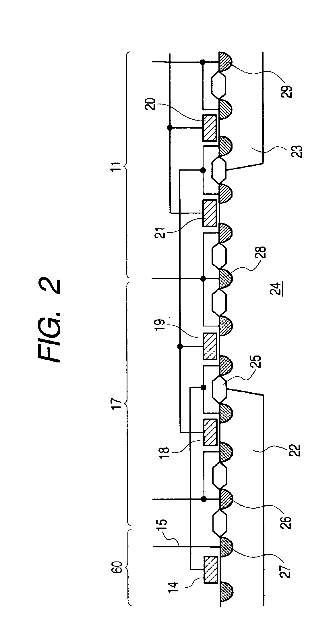
[0052]An equivalent circuit of a photoelectric conversion device of the embodiment is similar to the second embodiment of FIG. 4. However, the separation of the first and second N type wells and the separation of the first and second P type wells of the second embodiment are realized not based on PN junctions but based on insulating layer formation using a silicon on insulator (SOI) substrate and trench processing. FIG. 6 is a conceptual diagram showing a partial sectional structure of a select switch 60, a buffer circuit 40 and a vertical scanning circuit 6 of the embodiment. There is a semiconductor layer 57 on an insulating layer 56, and the select switch 60, the buffer circuit 40 and the vertical scanning circuit 6 are formed on the semiconductor layer 57.

[0053]The components are separated from one another in a horizontal direction by an insulating layer 58 of trench processing....


PUM


Abstract

A photoelectric conversion device formed on a single semiconductor substrate, including: a plurality of photoelectric conversion elements; a read-out circuit including a switch for reading out analog signals from the photoelectric conversion elements; a buffer circuit for driving the switch; and a logic circuit for processing digital signals. A first semiconductor area to which a ground level for the buffer circuit is supplied and a second semiconductor area to which a ground level for the logic circuit is supplied are electrically separated from each other.

Description

BACKGROUND OF THE INVENTION[0001]1. Field of the Invention[0002]The present invention relates to a photoelectric conversion device used for a scanner, a video camera, a digital still camera etc.[0003]2. Related Background Art[0004]In recent years, a photoelectric conversion device called a CMOS sensor provided using a CMOS process has been a focus of attention. Use of the CMOS sensor particularly in a field of portable information devices is expected because of its easy loading together with peripheral circuits, low voltage driving etc. FIG. 8 shows an equivalent circuit of a photoelectric conversion device according to a conventional art. In the drawing, pixels are arranged in 2×2 array, but the pixels are not particularly limited to this array. In FIG. 8, a unit pixel includes a photodiode 1 which is a photoelectric conversion element, an amplification metal oxide silicon field effect transistor (MOSFET) 2 for amplifying a signal generated at the pbotodiode 1, a reset switch 4 for...

Claims


Application Information

Patent Timeline
IPC IPC(8): H01L27/12H04N3/15H01L27/146H01L31/10H04N5/335H04N5/357H04N5/369H04N5/374
CPCH01L27/12H01L27/14609H01L27/14643H01L2924/0002H01L2924/00
Inventor HIYAMA, HIROKIKOIZUMI, TORUSAKURAI, KATSUHITOFUJIMURA, MASARU
Owner CANON KK
Why Eureka
Try Eureka