Semiconductor device and its production process

a technology of semiconductor devices and production processes, applied in semiconductor devices, semiconductor/solid-state device details, electrical devices, etc., can solve problems such as resistance rise, and achieve the effect of inhibiting the grain boundary diffusion of co atoms and preventing resistance ris

Inactive Publication Date: 2005-11-01
RENESAS ELECTRONICS CORP
View PDF15 Cites 22 Cited by
  • Summary
  • Abstract
  • Description
  • Claims
  • Application Information

AI Technical Summary

Benefits of technology

[0006]Rise of resistance of the cobalt silicide film is attributable to the insular coagulation of the cobalt silicide which occurs when the cobalt (Co) atoms composing the cobalt silicide film are diffused mostly along the crystal grain boundaries and recombined with silicon in a heat treatment at around 800° C. or above. Therefore, for preventing the rise of resistance due to the coagulation of cobalt silicide film, it is expedient to inhibit the diffusion of cobalt atoms in the cobalt silicide film.
[0007]On this concept, the present inventors disclosed that it is possible to inhibit the grain boundary diffusion of Co atoms in the cobalt silicide film when a specific element—an element having a smaller atomic radius than Co atom and specified by the fact that the inter-hetero-atomic energy between this element and Co element is not more than 20% smaller or greater than the inter-iso-atomic energy of Co element—is contained in said cobalt silicide film. That is, it was found the diffusion of Co atoms can be inhibited by containing nickel or iron element in the cobalt silicide film, and that in this case, the ratio of nickel or iron element to cobalt in said film should be preferably 0.05 to 50 atomic %, more preferably 0.05 to 18 atomic %.

Problems solved by technology

However, when the diffusion layer is made shallow and the cobalt silicide film is thinned with miniaturization of the semiconductor devices, there arises the new problem that the cobalt silicide coating, which was film-like when formed, is coagulated by a high-temperature heat treatment in, for instance, the capacitor forming step and takes a partially insular configuration, causing a rise of resistance.

Method used


Image

  • Semiconductor device and its production process
  • Semiconductor device and its production process
  • Semiconductor device and its production process

Examples


first embodiment

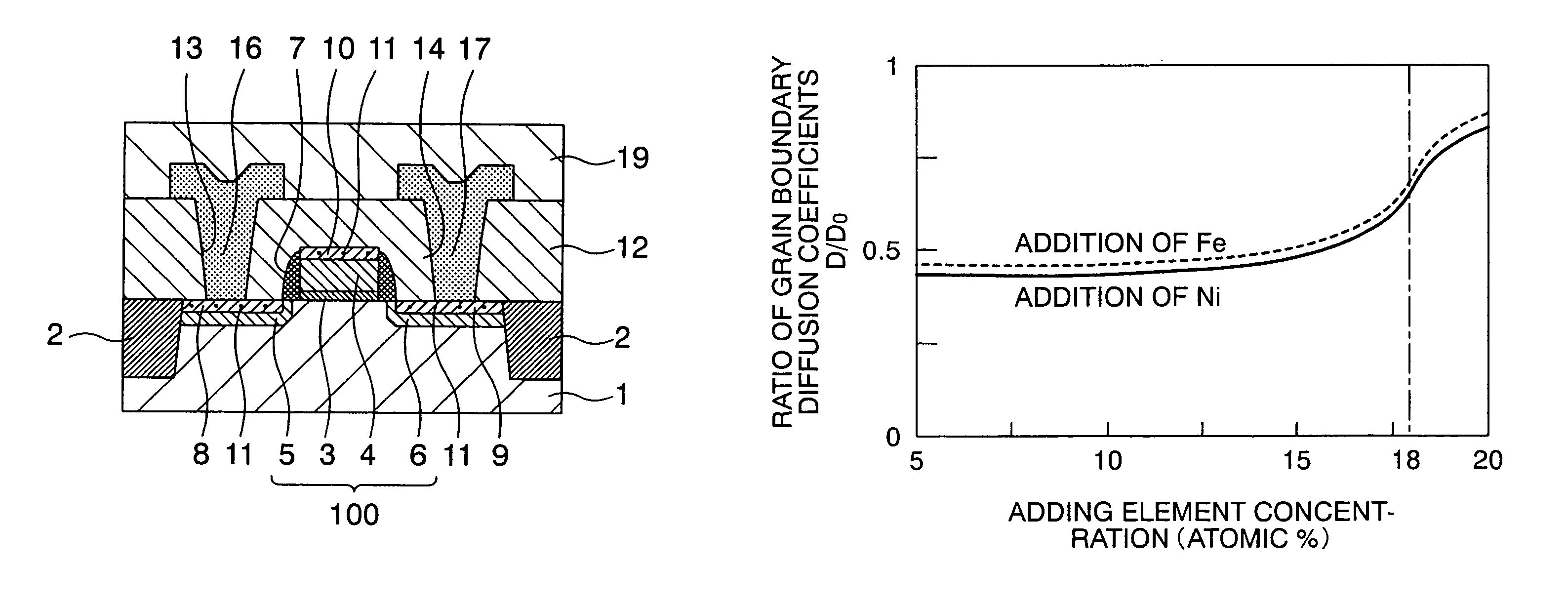
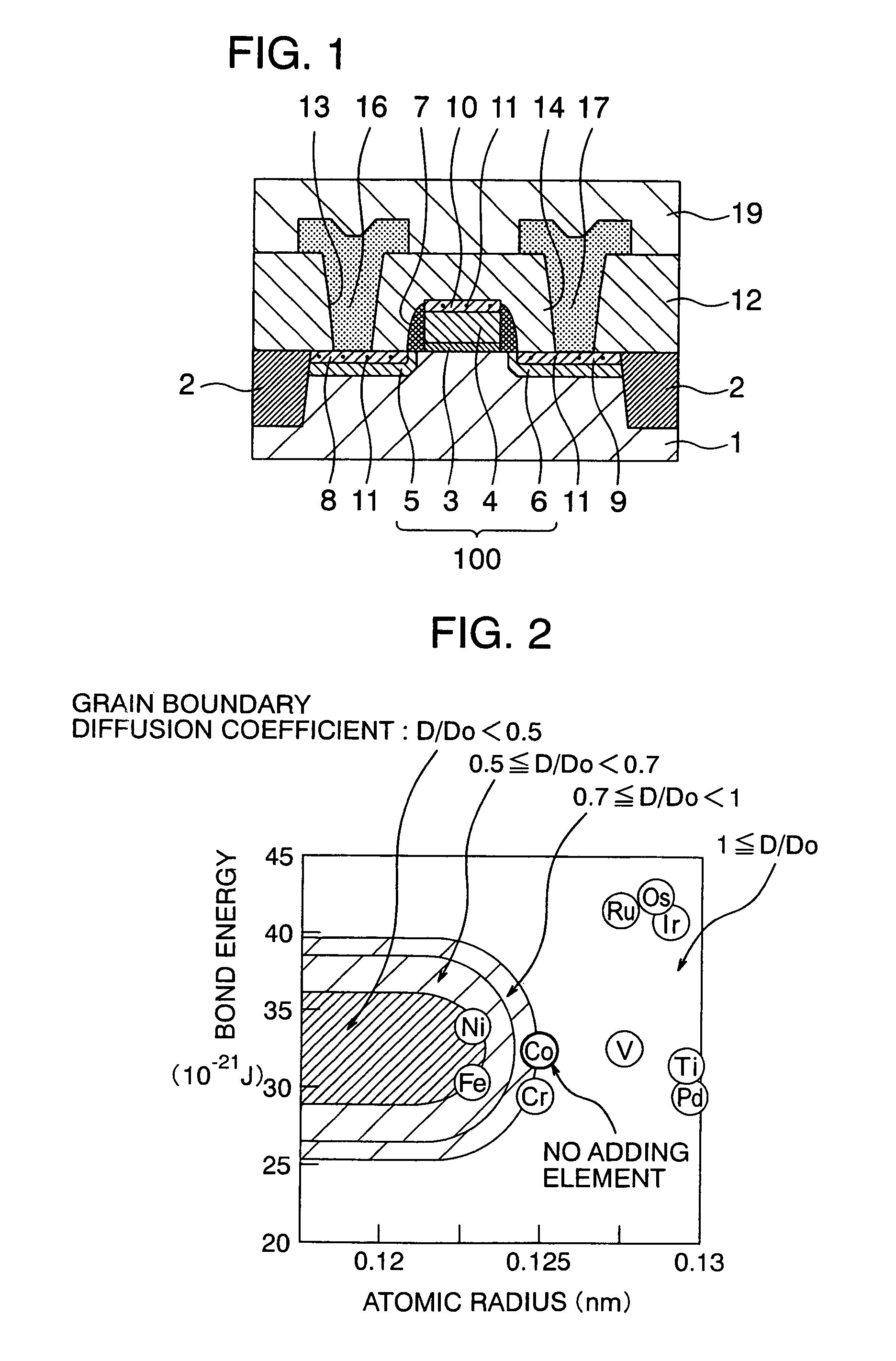
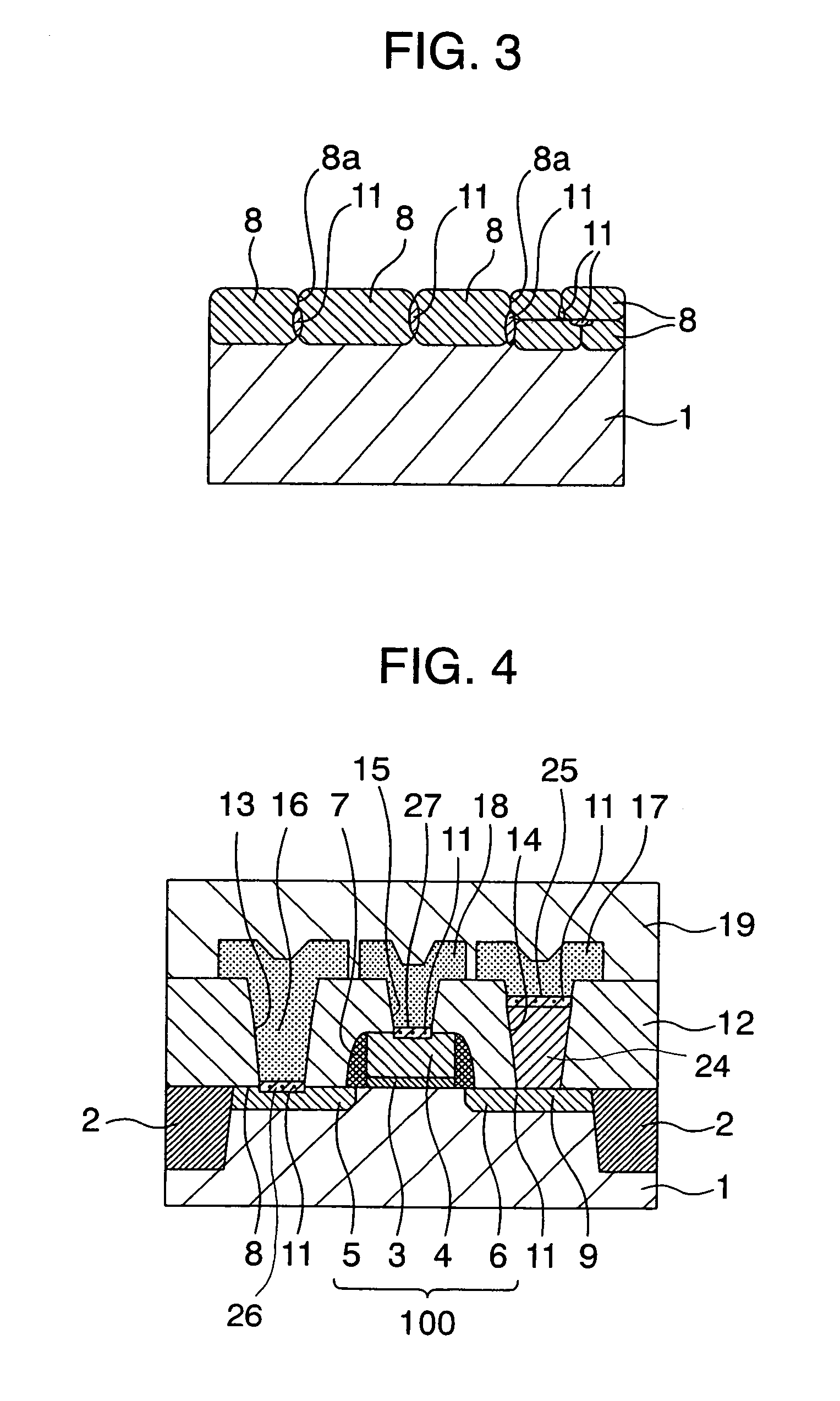
[0027]First, a sectional structure of a principal part of a semiconductor device in the present invention is shown in FIG. 1.

[0028]The semiconductor device according to this embodiment of the invention, as shown in FIG. 1, has MOS transistors 100 formed on the surface of a silicon substrate, each of said MOS transistors comprising a gate oxide film 3, a gate electrode 4 made of a polycrystalline silicon film, and a pair of diffusion layers 5, 6 (source and drain region). These MOS transistors are isolated by the isolating films 2. Said gate electrode 4 is made of a polycrystalline silicon film, a thin metal film, a metal silicide film or a laminate thereof. Side walls 7 are formed on both sides of said gate electrode 4. The gate oxide film 3 is made of, for instance, a silicon oxide film, a silicon nitride film, a ferroelectric film or a laminate thereof.

[0029]Cobalt silicide films 8, 9, 10 are formed on the gate electrode 4 and the diffusion layers 5, 6. Said cobalt silicide films ...

third embodiment

[0054]Next, the present invention is described with reference to FIG. 5.

[0055]FIG. 5 shows a sectional structure of a principal part of a semiconductor device according to this embodiment of the invention, in which the parts corresponding to those in the first embodiments are affixed the same reference numerals.

[0056]The semiconductor device according to this embodiment shown in FIG. 5 is a modification of the semiconductor device according to the first embodiment shown in FIG. 1. The difference of this embodiment from the first embodiment is that in this embodiment a capacitor 101 comprising a laminate of a lower electrode 28, a dielectric film 29 and an upper electrode 30 is provided on the insulating film 12 of the first layer.

[0057]The dielectric film 29 constituting part of the capacitor is made of, for instance, a silicon oxide film, a tantalum oxide film, a BST (barium strontium titanate) film, a PZT (zinc zirconate titanate) film or the like. The lower electrode 29 or upper ...

fourth embodiment

[0060]Now, the present invention is described with reference to FIG. 6.

[0061]FIG. 6 is a sectional structure of a principal part of a semiconductor device according to the present embodiment, in which the parts corresponding to those in the first or third embodiment are affixed the same reference numerals.

[0062]The semiconductor device according to the present embodiment shown in FIG. 6 is a modification of the semiconductor device according to the first embodiment shown in FIG. 1 and that according to the third embodiment. In the present embodiment, the semiconductor device according to the first embodiment and that according to the third embodiment are provided on a same silicon substrate 1. That is, the semiconductor device according to the present embodiment is of a structure in which memory unit 102 and CPU unit 103 are formed on a silicon substrate 1.

[0063]In this embodiment, too, said cobalt silicide films 8, 9, 10 contain at least one adding element 11, and at least one of s...


PUM

PropertyMeasurementUnit
concentrationaaaaaaaaaa
contact resistanceaaaaaaaaaa
resistanceaaaaaaaaaa

Abstract

In a semiconductor device having a cobalt silicide film, at least nickel or iron is contained in the cobalt silicide film for preventing the rise of resistance incidental to thinning of the film.

Description

CROSS REFERENCE TO RELATED APPLICATION[0001]This application is a divisional application of U.S. Ser. No. 09 / 787,743, filed Jun. 8, 2001, now U.S. Pat. No 6,686,274 the contents of which are incorporated herein by reference, which is a 371 application of International Application No. PCT / JP99 / 05108, filed Sep. 20, 1999.TECHNICAL FIELD[0002]The present invention relates to a semiconductor device and its production process, particularly to a semiconductor device having a cobalt silicide film and its production process.BACKGROUND ART[0003]With the recent trend toward higher integration and miniaturization of the semiconductor devices, reduction of contact resistance at the joint of metal wiring and silicon substrate has become essential for high-speed operation. Regarding the techniques for reducing contact resistance, for instance JP-A-08-78357 suggests to form a cobalt silicide film on the diffusion layer (source / drain) or polycrystalline silicon electrodes on a silicon substrate.DIS...

Claims


Application Information

Patent Timeline
Patent Type & Authority Patents(United States)
IPC IPC(8): H01L21/285H01L21/336H01L21/02H01L21/70H01L21/768
CPCH01L21/28518H01L21/76877H01L29/665H01L21/24
Inventor SHIMAZU, HIROMIIWASAKI, TOMIOOHTA, HIROYUKIMIURA, HIDEOIKEDA, SHUJI
Owner RENESAS ELECTRONICS CORP
Why Eureka
Try Eureka