

Optical devices with engineered nonlinear nanocomposite materials
a technology of nonlinear nanocomposite materials and optical devices, applied in nonlinear optics, instruments, nanoinformatics, etc., can solve the problems of high-speed electronic cores, complex, cumbersome, expensive, etc., and the complexity, size and expense of such optical-to-electronic-to-optical (oeo) components become even more problematic, and oeo devices are typically the rate-limiting component in an optical network
Inactive Publication Date: 2005-11-01
SAMSUNG ELECTRONICS CO LTD
View PDF171 Cites 74 Cited by
- Summary
- Abstract
- Description
- Claims
- Application Information
AI Technical Summary
Benefits of technology
These nanocomposite materials enhance the nonlinear optical properties, allowing for faster switching speeds and reduced device size, addressing the limitations of current technologies by providing a more efficient and cost-effective solution for high-speed optical data processing and transmission.
Problems solved by technology
Most current optical cross-connect systems comprise high-speed electronic cores, which are complex, cumbersome, and expensive.
The complexity, size, and expense of such optical-to-electronic-to-optical (OEO) components become even more problematic with higher bit-rates and port counts, even as the cost of electronic components decreases, due to cross-talk and RF transport issues.
OEO devices are typically the rate-limiting component in an optical network.
Many all-optical switching technologies are relatively slow and are therefore generally limited to static configuration control.
These relatively slow all-optical switches, however, are generally inadequate for fast switching applications such as dynamic packet switching (˜1 ns), optical modulation (˜100 ps), header reading in packet switched networks (<25 ps), and all-optical data-processing (<1 ps).
However, these devices are rapidly approaching their speed limits, as they rely on fast electronic signals in order to perform optical processing or modulation, and these electronic signals suffer increasingly greater losses due to the fundamental limitations of high-speed electrical propagation.
Of these nonlinear optical phenomena, χ(3) based phenomena have the most flexibility but currently suffer from a lack of practical materials with both high nonlinearity and relatively low loss.
Due to the small γ of silica, however, impractical fiber lengths (˜1000 km) are required for these devices to operate at typical telecommunication powers (˜10 mW).
While this technology is extremely advanced in the field of microelectronics, it is still in its infancy with respect to optics.
For instance, for χ(2) based devices, crystalline LiNiO3 cannot be arbitrarily inserted within a waveguide created by these techniques.
In addition, polymeric nonlinear materials, which are more easily processed, typically have values for χ(3) that are too low for efficient switching.
While proof-of-concept for all-optical switches based on SOAs has been shown, problems with amplified spontaneous emission buildup currently make cascading many of these switches problematic.
In addition, the materials used for SOAs (typically InP) are expensive and create inherent difficulties with coupling to standard silica fibers and waveguides.
Photonic bandgap materials are another promising approach, but manufacturing using the previously proposed materials is still beyond current practical capabilities.
Finally, new nonlinear crystalline materials have been developed (e.g. periodically poled LiNbO3 and p-toluene sulphonate (PTS)) but are typically expensive and difficult to process, making incorporation into waveguide devices problematic.
Nonlinear polymers, with more appealing mechanical properties, have also been developed, but problems such as kinks in the polymer chains can limit the maximum nonlinearity to a value still unsuitable for practical all-optical applications.
In cases where highly nonlinear polymers have been produced (e.g., polyacetylene), many of the appealing mechanical properties are lost, creating problems similar to those found in crystalline materials.
As such, it has been extremely difficult to find a practical material that simultaneously satisfies various requirements for a commercial χ(3) based nonlinear device.
While many materials may have one or more of these desirable characteristics, at present, no single material comprises a sufficient number of these characteristics required for an optimal χ(3) based optical switch.
In fact, besides SOAs, no commercial devices are currently available, primarily due to a lack of appropriate nonlinear optical materials.
Method used
View moreImage
Smart ImageViewing Examples

Examples
example 9
[0303]The preparation of Example 1 is repeated using allylmagnesium bromide as the capping agent.
example 10
[0304]The preparation of Example 1 is repeated using 4-methoxyphenylithium as the capping agent.
example 11
[0305]The preparation of Example 1 is repeated using pentafluorophenyllithium as the capping agent.
Login to View More PUM
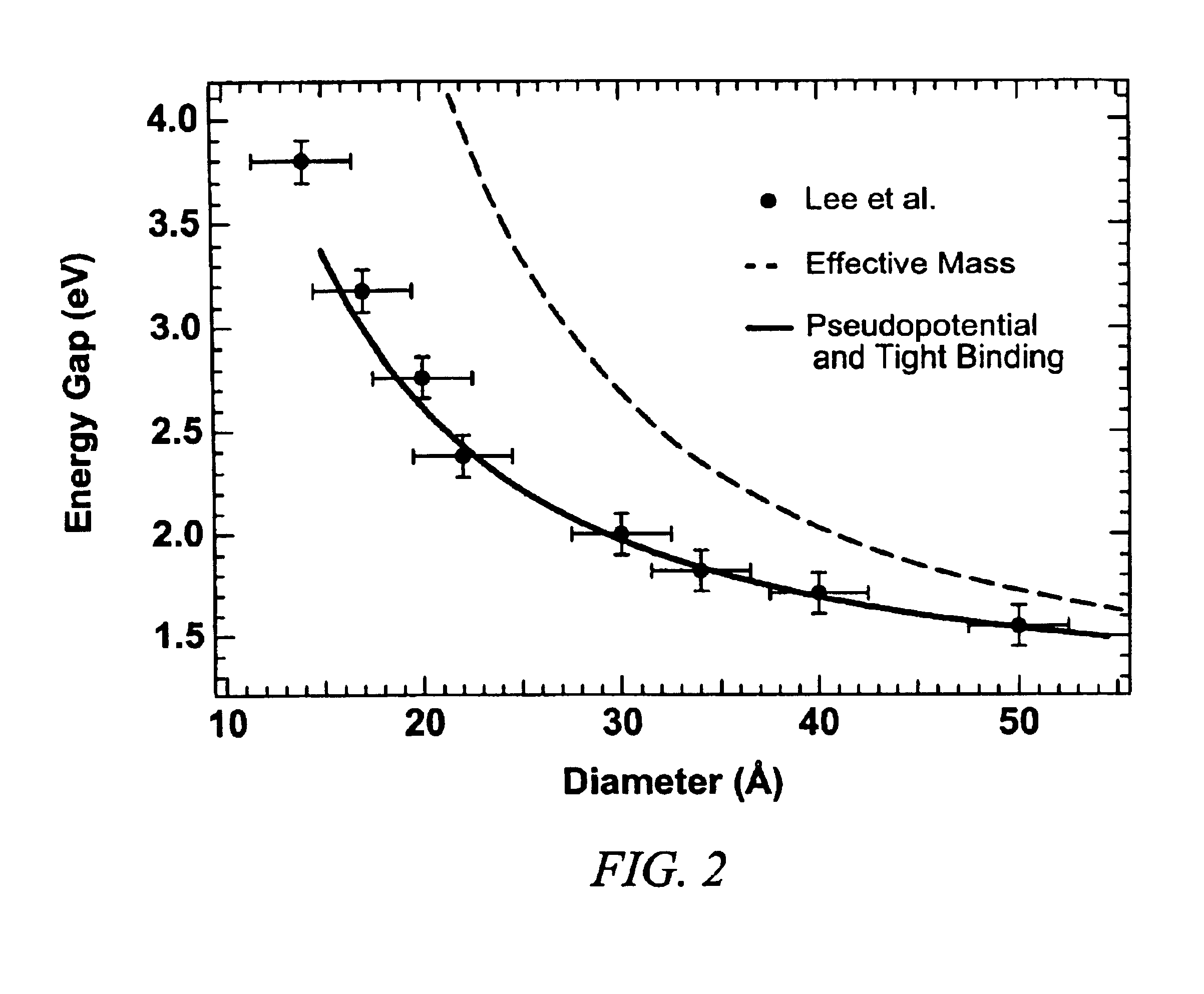
| Property | Measurement | Unit |
|---|---|---|
| sizes | aaaaa | aaaaa |
| quantum efficiency | aaaaa | aaaaa |
| diameter | aaaaa | aaaaa |
Abstract
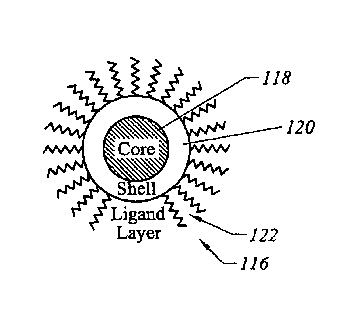
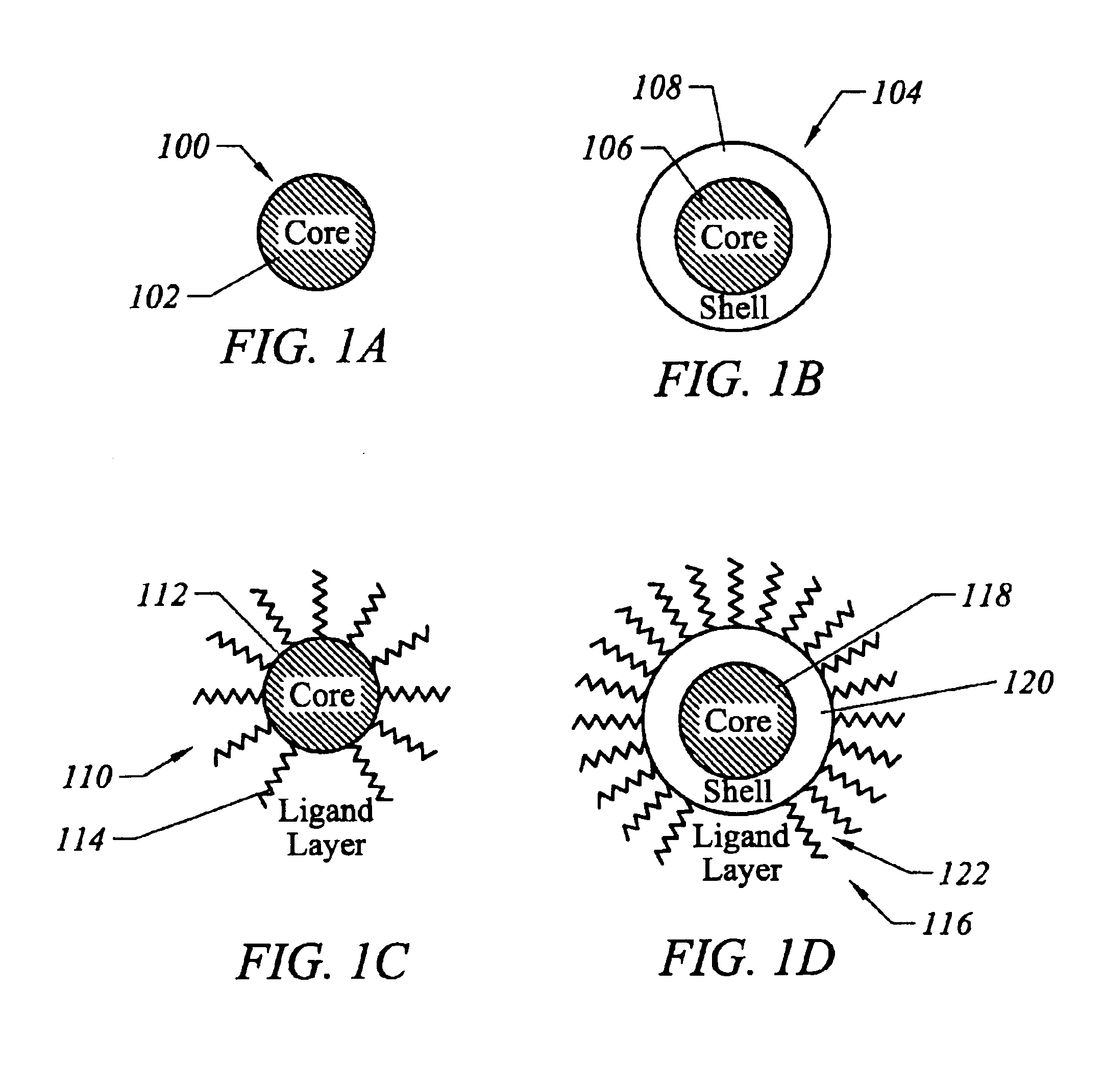
The invention relates to an optical device. The optical device comprises a waveguide core and a nanocomposite material optically coupled to the waveguide core. The nanocomposite material includes a plurality of quantum dots. The nanocomposite material has a nonlinear index of refraction γ that is at least 10−9 cm2 / W when irradiated with an activation light having a wavelength λ between approximately 3×10⁻⁵ cm and 2×10⁻⁴ cm.
Description
CROSS-REFERENCE TO RELATED APPLICATIONS[0001]This application is a divisional of U.S. patent application Ser. No. 10 / 211,991, filed on Aug. 2, 2002 now U.S. Pat. No. 6,819,845, which claims the benefit of U.S. Provisional Application Ser. No. 60 / 309,898, filed on Aug. 2, 2001, U.S. Provisional Application Ser. No. 60 / 309,905, filed on Aug. 2, 2001, U.S. Provisional Application Ser. No. 60 / 309,979, filed on Aug. 2, 2001, U.S. Provisional Application Ser. No. 60 / 310,090, filed on Aug. 2, 2001, and U.S. Provisional Application Ser. No. 60 / 310,095, filed on Aug. 2, 2001, the disclosures of which are incorporated herein by reference in their entirety.FIELD OF THE INVENTION[0002]This invention relates generally to optical devices. More particularly, this invention relates to optical devices comprising engineered nonlinear nanocomposite materials.BACKGROUND OF THE INVENTION[0003]As telecommunication networks continue to expand their need for bandwidth, it is becoming increasingly necessary...
Claims
Login to View More Application Information
Patent Timeline
 Patent Type & AuthorityPatents(United States)
IPC IPC(8): G02F1/355G02F1/35G02B6/122H01L29/12H01L29/02G02F1/017G02F1/01G02B6/12G02F2/00G02F1/365H01L21/02H01L21/20H01L29/16H01L33/00H01L33/20H01L33/34
CPCB82Y10/00C25F3/12G02B6/122G02B6/1225G02F1/3515G02F1/3556H01L29/127B82Y20/00Y10S977/834G02B6/356G02B2006/12097G02B2006/12145G02B2006/12147G02B2006/12159G02B2006/12195G02F1/3517G02F1/3521G02F1/365G02F2001/01791G02F2001/217G02F2002/006G02F2202/32G02F2202/36H01L29/16H01L29/1602H01L33/20H01L33/34G02F1/01791G02F1/217G02F2/006
InventorLEE, HOWARD WING HOONCHIN, ALAN HAPPFENNINGER, WILLIAM MATTHEW
OwnerSAMSUNG ELECTRONICS CO LTD