Multi-chip package having a contiguous heat spreader assembly

a heat spreader and integrated circuit technology, applied in the direction of semiconductor devices, semiconductor/solid-state device details, electrical apparatus, etc., can solve the problems of increasing parasitics, requiring higher drive currents, and increasing power dissipation, so as to achieve greater thermal resistance elements, greater thermal transfer efficiency, and greater thermal transfer

Inactive Publication Date: 2005-11-08
BELL NORTHERN RES LLC
View PDF8 Cites 5 Cited by
  • Summary
  • Abstract
  • Description
  • Claims
  • Application Information

AI Technical Summary

Benefits of technology

[0014]According to another embodiment, a space is purposely left between integrated circuits. The space is dimensioned in order to accommodate one or more passive devices. While underfill material can be inserted and thereafter cured only in the region around the bonding pad interfaces, the space between neighboring integrated circuits is purposely void of any dielectric material, such as injected molded material or non-injected molded material. If a passive device is contained within that space, then the passive device will, in most instances, have an upper elevation that is not coplanar with an upper elevation of a packaged or unpackaged integrated circuit. This disparity in elevation will accommodate a heat spreader to be placed on the exposed upper surfaces of the integrated circuits with a space left between the heat spreader and any underlying passive devices. The space beneficially allows greater thermal transfer at the underneath surface of the heat spreader between neighboring integrated circuits and above any passive devices within that space.
[0015]If the multi-chip package connotes both unpackaged and packaged integrated circuits, the packaged integrated circuit may be thicker than the unpackaged integrated circuit. The heat spreader may, therefore, extend in two planes onto the exposed upper surfaces of those integrated circuits. Alternatively, the thinner unpackaged integrated circuit may have a second heat spreader placed between the unpackaged integrated circuit and the heat spreader. The second heat spreader preferably has an upper surface that is coplanar with the upper surface of a packaged integrated circuit so that a single, planar heat spreader can extend across all upper surfaces without having to be deformed, bent, or curved in any way so as to form two planes.
[0016]By using a heat spreader and purposely applying an air-filled gap or space between neighboring integrated circuits, greater thermal transfer efficiency can be obtained. The operating temperature of the multi-chip package is, therefore, governed by the temperature of the ambient surrounding the package, the amount of electrical power dissipation by the package, and the sum of thermal resistances of the elements and interfaces along a heat transfer path from the various integrated circuits to the ambient. By maintaining an air gap between integrated circuits, without a higher thermal resistance element in the interim, the heat transfer path from the upper and sidewalls of each integrated circuit is substantially enhanced. Moreover, by maintaining, for example, the memory and logic integrated circuits in close proximity to one another, the amount of electrical drive needed to power each chip is reduced and, accordingly, the electrical power dissipation within the overall multi-chip package is minimized. Still further, by placing the memory integrated circuit within a package, and then bonding the package to the substrate along with unpackaged logic circuits, a defective memory can be readily removed and replaced without having to discard the entire multi-chip package, for example.

Problems solved by technology

Packaging each integrated separately (whether by flip-chip or wire-bonding) and then placing the individual packaged integrated circuits on a printed circuit board not only increases the parasitics, but also requires higher drive currents, higher power dissipation, more routing congestion, and leads to a larger overall size.
This, however, would lead to a relatively high lead time and design complexity of that integrated circuit, and result in a larger overall integrated circuit size.

Method used


Image

  • Multi-chip package having a contiguous heat spreader assembly
  • Multi-chip package having a contiguous heat spreader assembly
  • Multi-chip package having a contiguous heat spreader assembly

Examples


Embodiment Construction

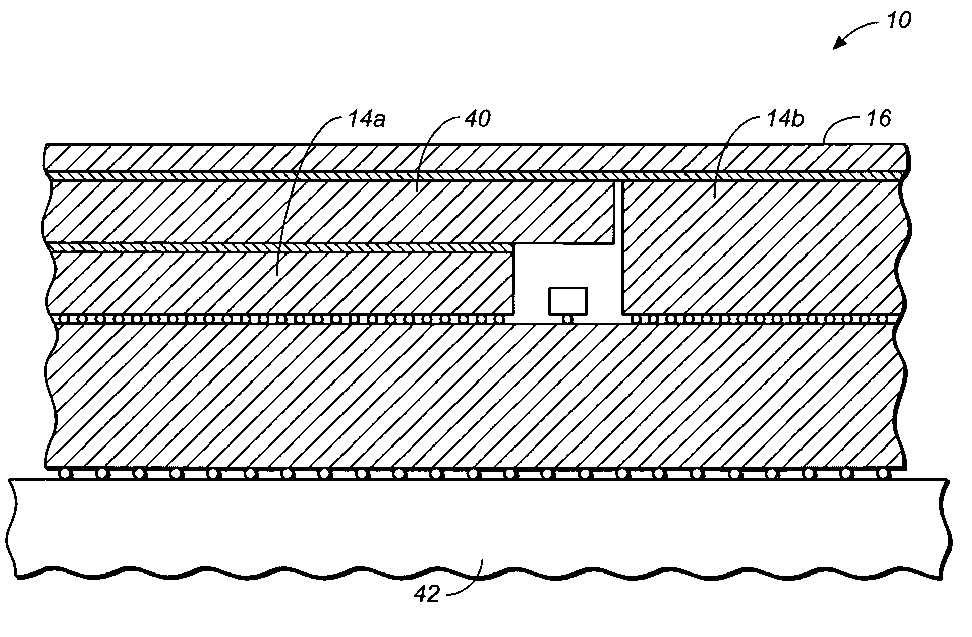
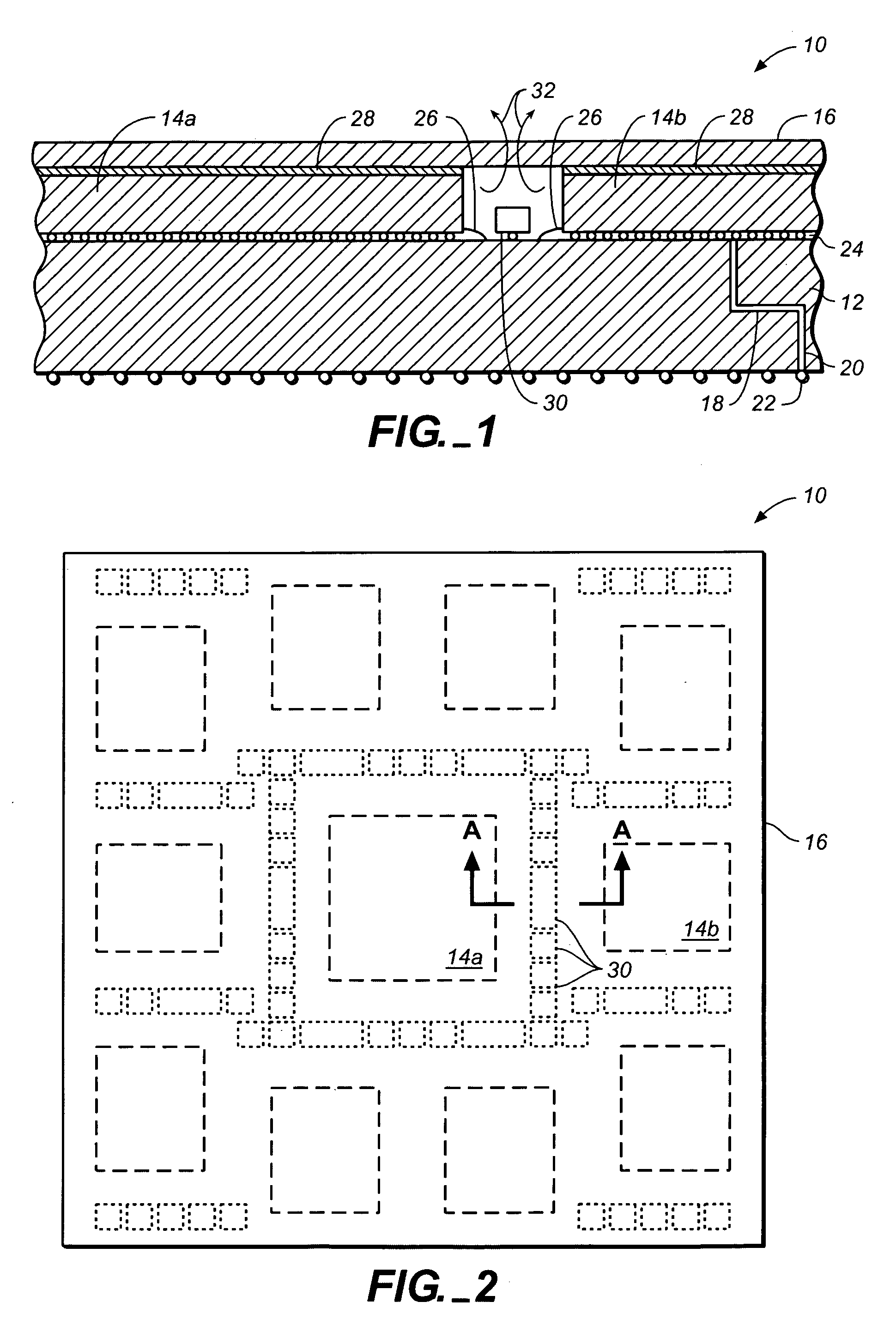
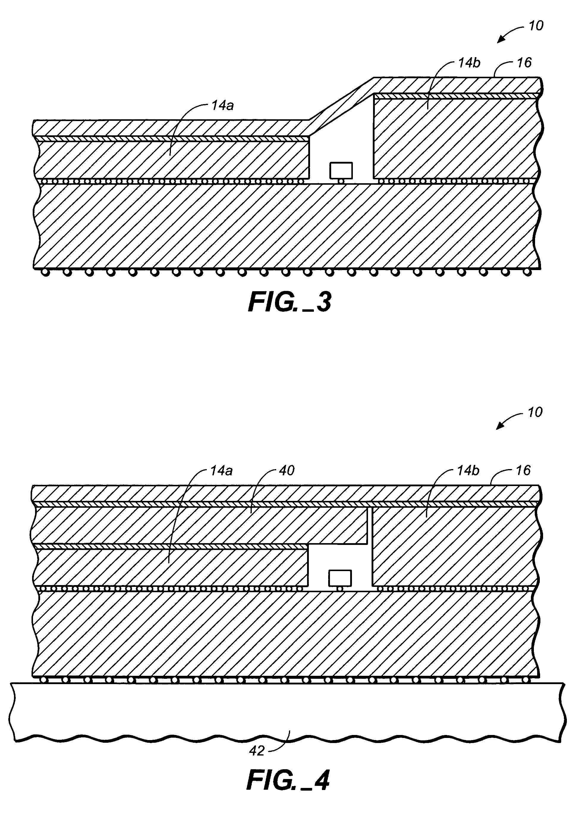
[0023]Turning now to FIG. 1, a portion of a multi-chip package 10 is shown along plane A—A of FIG. 2. Package 10 includes a multi-layer substrate 12, two or more integrated circuits 14 placed on substrate 12, and a heat spreader 16 placed on the integrated circuits 14. Substrate 12 preferably includes multiple layers of conductive elements separated by a dielectric material. The process steps in forming a multi-layer substrate 12 is generally well known. For example, the dielectric material may comprise multiple grades of epoxy resins supported on woven glass fabric. The material is often referred to as a fiberglass-epoxy material. Alternatively, the material can be made of ceramic (e.g., aluminum oxide, alumina, Al2O3, or aluminum nitride). Still further, the material can be made of organics, such as polymide or Teflon®. The epoxy materials or resins can be G-10 or FR-4 grades of epoxy resins, if desired.

[0024]The conductive layers can be made of any electrically conductive materia...


PUM


Abstract

A system and method are provided for forming a multi-chip package. The multi-chip package includes a multi-layer substrate and a heat spreader of single, unibody construction. At least two integrated circuits are coupled between the multi-layer substrate and the heat spreader. The integrated circuits are spaced from one another to allow airflow between those circuits and a portion of the underside surface of the heat spreader. Depending on the layout of the package, a passive device can also be placed in the space between integrated circuits. The passive device extends upward a spaced distance from the underneath surface of the heat spreader so as not to block the airflow therebetween. The multi-chip package can accommodate integrated circuits that are either all packaged, all unpackaged, or a combination of each. If packaged and unpackaged integrated circuits are placed on the multi-layer substrate, the heat spreader can extend in two separate planes to accommodate the different thicknesses of those packaged and unpackaged integrated circuits. Alternatively, a second heat spreader can be placed on a relatively thin integrated circuit so that the upper surface of the second heat spreader is coplanar with an upper surface of a relatively thick integrated circuit. This will allow a planar heat spreader to be arranged across the thick integrated circuit and the second heat spreader. In all instances, however, the heat spreader extends as a single, contiguous unibody element across the entire multi-chip package.

Description

BACKGROUND OF THE INVENTION[0001]1. Field of Invention[0002]This invention relates to integrated circuit packaging and, more particularly, to multiple integrated circuits secured to a substrate and having a heat spreader thermally coupled to a surface of each of the integrated circuits opposite the surface to which the substrate is secured.[0003]2. Description of Related Art[0004]The following descriptions and examples are not admitted to be prior art by virtue of their inclusion within this section.[0005]An integrated circuit is generally manufactured by processing a topography of a wafer. Multiple processing steps take place in order to form circuitry across the processed surface. Following manufacture, individual die or chips are drawn from the wafer by slicing the wafer along the scribe line between neighboring die.[0006]Each integrated circuit (i.e., die or chip) includes a series of input / output bonding pads arranged on the upper surface of the integrated circuit. The bonding ...

Claims


Application Information

Patent Timeline
Patent Type & Authority Patents(United States)
IPC IPC(8): H01L23/02H01L23/34H01L23/10H01L23/36H01L25/065
CPCH01L23/36H01L25/0655H01L2924/15153H01L2924/1517H01L2924/15311H01L2924/16195H01L2224/16225H01L2224/32245H01L2224/73253H01L2924/19105
Inventor EVANS, THOMASMIHELCIC, STANMILLER, LEAH M.NAGARAJAN, KUMARFULCHER, EDWIN M.
Owner BELL NORTHERN RES LLC
Why Eureka
Try Eureka